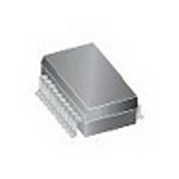
49FCT805BTSO IDT, Integrated Device Technology Inc, 49FCT805BTSO Datasheet - Page 5

49FCT805BTSO
Manufacturer Part Number
49FCT805BTSO
Description
Manufacturer
IDT, Integrated Device Technology Inc
Datasheet
1.49FCT805BTSO.pdf
(7 pages)
Specifications of 49FCT805BTSO
Number Of Outputs
10
Operating Supply Voltage (max)
5.5V
Operating Temp Range
0C to 70C
Propagation Delay Time
6ns
Operating Supply Voltage (min)
4.5V
Mounting
Surface Mount
Pin Count
20
Operating Supply Voltage (typ)
5V
Package Type
SOIC
Quiescent Current
5uA
Operating Temperature Classification
Commercial
Lead Free Status / Rohs Status
Not Compliant
Available stocks
Company
Part Number
Manufacturer
Quantity
Price
Part Number:
49FCT805BTSO
Manufacturer:
SDT
Quantity:
20 000
NOTES:
1. t
2. Propagation delay range indicated by Min. and Max. limit is dues to Vcc, operating temperature, and process parameters. These propagation delay limits do not imply
3. See Test Circuits and Waveforms.
4. Minimum limits are guaranteed but not tested on Propagation Delays.
SWITCHING CHARACTERISTICS OVER OPERATING RANGE - MILITARY
NOTES:
1. t
2. Propagation delay range indicated by Min. and Max. limit is dues to Vcc, operating temperature, and process parameters. These propagation delay limits do not imply
3. See Test Circuits and Waveforms.
4. Minimum limits are guaranteed but not tested on Propagation Delays.
SWITCHING CHARACTERISTICS OVER OPERATING RANGE - COMMERCIAL
IDT49FCT805BT/CT
FAST CMOS BUFFER/CLOCK DRIVER
Symbol
Symbol
t
t
t
SK(PP)
t
t
t
SK(PP)
SK(O)
SK(P)
t
t
skew.
skew.
t
t
t
t
t
t
SK(O)
SK(P)
t
t
t
t
PZH
PHZ
PLH
PLH
PHL
PZL
PLZ
PLH
PHL
PZH
PHZ
PLH
PZL
PLZ
t
t
t
t
R
F
R
F
, t
, t
PHL
PHL
, and t
, and t
Parameter
Propagation Delay
IN
Output Rise Time
Output Fall Time
Output skew: skew between outputs of all banks of
same package (inputs tied together)
Pulse skew: skew between opposite transitions
of same output (|t
Part-to-part skew: skew between outputs of different
packages at same power supply voltage,
temperature, package type and speed grade
Output Enable Time
OE
Output Disable Time
OE
A
A
A
A
A
A
SK
SK
to OAx, IN
to OAx, IN
to OAx, OE
to OAx, OE
to OAx, OE
to OAx, OE
(pp) are production tested. All other parameters are guaranteed but not production tested.
(pp) are production tested. All other parameters are guaranteed but not production tested.
B
B
PHL -–
PHL -–
to OBx
B
B
B
B
to OBx
to OBx
to OBx
to OBx
to OBx
t
t
PLH
PLH
|)
|)
Conditions
Conditions
R
R
C
C
L
L
L
L
= 500Ω
= 50pF
= 500Ω
= 50pF
(3)
(3)
5
Min
Min
1.5
1.5
1.5
1.5
1.5
1.5
—
—
—
—
—
—
—
—
—
—
.
MILITARY AND COMMERCIAL TEMPERATURE RANGES
.
(4)
(4)
FCT805BT
FCT805BT
Max
Max
5.7
1.5
0.9
0.9
1.5
6.5
6.5
1.5
1.5
0.7
0.7
1.2
2
5
6
6
.
.
Min
Min
1.5
1.5
1.5
1.5
1.5
1.5
—
—
—
—
—
—
—
—
—
—
.
.
(4)
(4)
FCT805CT
FCT805CT
Max
Max
5.2
1.5
0.7
0.8
1.2
4.5
1.5
1.5
0.5
0.6
2
6
6
1
5
5
.
.
(1,2)
Unit
Unit
ns
ns
ns
ns
ns
ns
ns
ns
ns
ns
ns
ns
ns
ns
ns
ns
(1,2)


