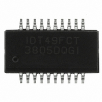
IDT49FCT3805DQGI IDT, Integrated Device Technology Inc, IDT49FCT3805DQGI Datasheet

IC CLK DVR 3.3V DUAL 1:5 20-QSOP

IDT49FCT3805DQGI

Manufacturer Part Number
IDT49FCT3805DQGI
Description
IC CLK DVR 3.3V DUAL 1:5 20-QSOP
Manufacturer
IDT, Integrated Device Technology Inc
Series
49FCTr
Type
Fanout Buffer (Distribution)r
Datasheet

Specifications of IDT49FCT3805DQGI

Number Of Circuits
2
Ratio - Input:output
1:5
Differential - Input:output
No/No
Input
LVTTL
Output
LVTTL
Frequency - Max
133MHz
Voltage - Supply
3 V ~ 3.6 V
Operating Temperature
-40°C ~ 85°C
Mounting Type
Surface Mount
Package / Case
20-QSOP
Frequency-max
133MHz
Number Of Outputs
10
Operating Supply Voltage (max)
3.6V
Operating Temp Range
-40C to 85C
Propagation Delay Time
3ns
Operating Supply Voltage (min)
3V
Mounting
Surface Mount
Pin Count
20
Operating Supply Voltage (typ)
3.3V
Package Type
QSOP
Input Frequency
166MHz
Operating Temperature Classification
Industrial
Lead Free Status / RoHS Status
Lead free / RoHS Compliant
Other names
49FCT3805DQGI
800-1346
800-1346-5
800-1346

Available stocks

Company
Part Number
Manufacturer
Quantity
Price
Part Number:
IDT49FCT3805DQGI
Manufacturer:
IDT
Quantity:
20 000
Company:
Part Number:
IDT49FCT3805DQGI8
Quantity:
2 143
Company:
Part Number:
IDT49FCT3805DQGI8
Quantity:
2 243
Company:
Part Number:
IDT49FCT3805DQGI8
Quantity:
2 243
FUNCTIONAL BLOCK DIAGRAM
INDUSTRIAL TEMPERATURE RANGE
FEATURES:
• Advanced CMOS Technology
• Guaranteed low skew < 200ps (max.)
• Very low propagation delay < 2.5ns (max)
• Very low duty cycle distortion < 270ps (max)
• Very low CMOS power levels
• Operating frequency up to 166MHz
• TTL compatible inputs and outputs
• Inputs can be driven from 3.3V or 5V components
• Two independent output banks with 3-state control
• 1:5 fanout per bank
• "Heartbeat" monitor output
• V
• Available in SSOP and QSOP packages
The IDT logo is a registered trademark of Integrated Device Technology, Inc.
IDT49FCT3805D/E
3.3V CMOS DUAL 1-TO-5 CLOCK DRIVER
c
OE
OE
IN
IN
CC
A
B
A
B
2004 Integrated Device Technology, Inc.
= 3.3V ± 0.3V
5
5
3.3V CMOS DUAL
1-TO-5 CLOCK DRIVER
OA
OB
M O N
1
1
- OA
- OB
5
5
1
DESCRIPTION:
technology. The device consists of two banks of drivers, each with a 1:5 fanout
and its own output enable control. The device has a "heartbeat" monitor for
diagnostics and PLL driving. The MON output is identical to all other outputs
and complies with the output specifications in this document. The FCT3805 offers
low capacitance inputs.
quality and skew are critical. The FCT3805 also allows single point-to-point
transmission line driving in applications such as address distribution, where one
signal must be distributed to multiple recievers with low skew and high signal
quality.
frequencies on bank A and B, please see AN-236.
PIN CONFIGURATION
The FCT3805 is a 3.3 volt clock driver built using advanced CMOS
The FCT3805 is designed for high speed clock distribution where signal
For more information on using the FCT3805 with two different input
GND
GND
V
OA
OA
OA
OA
OE
OA
CCA
IN
Q
A
A
A
1
2
4
5
3
1
2
3
4
5
6
7
8
9
10
SSOP/ QSOP
INDUSTRIAL TEMPERATURE RANGE
TOP VIEW
IDT49FCT3805D/E
20
19
18
17
16
15
14
13
12
11
V
OB
OB
OB
GND
OB
OB
MON
OE
IN
CCB
B
1
2
3
4
5
B
MAY 2010
B
DSC-5864/19

Related parts for IDT49FCT3805DQGI

IDT49FCT3805DQGI Summary of contents

Page 1

IDT49FCT3805D/E 3.3V CMOS DUAL 1-TO-5 CLOCK DRIVER FEATURES: • Advanced CMOS Technology • Guaranteed low skew < 200ps (max.) • Very low propagation delay < 2.5ns (max) • Very low duty cycle distortion < 270ps (max) • Very low CMOS ...

Page 2

IDT49FCT3805D/E 3.3V CMOS DUAL 1-TO-5 CLOCK DRIVER ABSOLUTE MAXIMUM RATINGS Symbol Description V Input Power Supply Voltage CC V Input Voltage I V Output Voltage O T Junction Temperature J T Storage Temperature STG NOTE: 1. Stresses greater than those ...

Page 3

IDT49FCT3805D/E 3.3V CMOS DUAL 1-TO-5 CLOCK DRIVER POWER SUPPLY CHARACTERISTICS Symbol Parameter I Quiescent Power Supply Current CCL I CCH I CCZ ∆I Power Supply Current per Input HIGH CC I Dynamic Power Supply Current CCD (3) per Output I ...

Page 4

IDT49FCT3805D/E 3.3V CMOS DUAL 1-TO-5 CLOCK DRIVER SWITCHING CHARACTERISTICS OVER OPERATING RANGE - 3805D Symbol Parameter t Propagation Delay PLH OAn OBn PHL Output Rise Time (0. Output ...

Page 5

IDT49FCT3805D/E 3.3V CMOS DUAL 1-TO-5 CLOCK DRIVER TEST CIRCUITS AND WAVEFORMS Pulse Generator Pulse D.U.T Generator 15pF Test Circuit L SWITCH POSITION Test Disable Low Enable Low Disable High Enable High V ...

Page 6

IDT49FCT3805D/E 3.3V CMOS DUAL 1-TO-5 CLOCK DRIVER TEST CIRCUITS AND WAVEFORMS ENABLE DISABLE CONTROL INPUT t PZL V OUTPUT OH SW ITCH NORMALLY 1.5V CLOSED LOW t t PHZ PZH OUTPUT SW ITCH NORMALLY 1.5V OPEN HIGH V OL Enable ...

Page 7

IDT49FCT3805D/E 3.3V CMOS DUAL 1-TO-5 CLOCK DRIVER ORDERING INFORMATION XXXX X IDT49FCT Device Type Package CORPORATE HEADQUARTERS 6024 Silver Creek Valley Road San Jose, CA 95138 X Process -40°C to +85°C (Industrial) I Shrink Small Outline IC PY SSOP - ...

Related keywords