MC74HC595AD ON Semiconductor, MC74HC595AD Datasheet
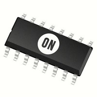
Counter Shift Registers 8-Bit 3 State Shift

MC74HC595AD

Manufacturer Part Number
MC74HC595AD
Description
Counter Shift Registers 8-Bit 3 State Shift
Manufacturer
ON Semiconductor
Datasheet

Specifications of MC74HC595AD

Counting Sequence
Serial to Serial/Parallel
Number Of Circuits
2
Package / Case
SOIC-16
Logic Family
74HC
Logic Type
CMOS
Output Type
3-State
Propagation Delay Time
140 ns, 100 ns, 28 ns, 24 ns
Supply Voltage (max)
6 V
Maximum Operating Temperature
+ 125 C
Minimum Operating Temperature
- 55 C
Function
Shift Register
Mounting Style
SMD/SMT
Operating Supply Voltage
2 V to 6 V
Dc
N/A
Lead Free Status / Rohs Status
No RoHS Version Available

Available stocks

Company
Part Number
Manufacturer
Quantity
Price
Part Number:
MC74HC595AD
Manufacturer:
MOTOROLA
Quantity:
422
Part Number:
MC74HC595AD
Quantity:
8 000
Part Number:
MC74HC595AD
Manufacturer:
ON/安森美
Quantity:
20 000
Company:
Part Number:
MC74HC595ADG
Quantity:
2 600
Company:
Part Number:
MC74HC595ADH
Quantity:
16
Part Number:
MC74HC595ADR2
Manufacturer:
ON/安森美
Quantity:
20 000
Part Number:
MC74HC595ADR2G
Quantity:
200 000
Part Number:
MC74HC595ADR2G
Manufacturer:
ON/安森美
Quantity:
20 000
Part Number:
MC74HC595ADR2G
0
Company:
Part Number:
MC74HC595ADR2G
Quantity:
65
Company:
Part Number:
MC74HC595ADR2G
Quantity:
25 000
Company:
Part Number:
MC74HC595ADR2G
Quantity:
50 000
Part Number:
MC74HC595ADTG
Manufacturer:
ON
Quantity:
9 400
Part Number:
MC74HC595ADTR2G
Manufacturer:
TDK
Quantity:
20 000
Part Number:
MC74HC595ADTR2G
Manufacturer:
ON/安森美
Quantity:
20 000
MC74HC595A
8-Bit Serial-Input/Serial or
Parallel-Output Shift
Register with Latched
3-State Outputs
High−Performance Silicon−Gate CMOS
D−type latch with three−state parallel outputs. The shift register
accepts serial data and provides a serial output. The shift register also
provides parallel data to the 8−bit latch. The shift register and latch
have independent clock inputs. This device also has an asynchronous
reset for the shift register.
CMOS MPUs and MCUs.
Features
*For additional information on our Pb−Free strategy and soldering details, please
© Semiconductor Components Industries, LLC, 2011
May, 2011 − Rev. 12
download the ON Semiconductor Soldering and Mounting Techniques
Reference Manual, SOLDERRM/D.
The MC74HC595A consists of an 8−bit shift register and an 8−bit
The HC595A directly interfaces with the SPI serial data port on
Standard No. 7A
Output Drive Capability: 15 LSTTL Loads
Outputs Directly Interface to CMOS, NMOS, and TTL
Operating Voltage Range: 2.0 to 6.0 V
Low Input Current: 1.0 mA
High Noise Immunity Characteristic of CMOS Devices
In Compliance with the Requirements Defined by JEDEC
Chip Complexity: 328 FETs or 82 Equivalent Gates
Improvements over HC595
Pb−Free Packages are Available*
− Improved Propagation Delays
− 50% Lower Quiescent Power
− Improved Input Noise and Latchup Immunity
1
16
16
See detailed ordering and shipping information in the package
dimensions section on page 2 of this data sheet.
16
1
(Note: Microdot may be in either location)
1
1
A
WL, L
YY, Y
WW, W
G, G
ORDERING INFORMATION
http://onsemi.com
CASE 751B
CASE 948F
DT SUFFIX
TSSOP−16
CASE 648
N SUFFIX
D SUFFIX
SOIC−16
PDIP−16
= Assembly Location
= Wafer Lot
= Year
= Work Week
= Pb−Free Package
Publication Order Number:
16
16
1
1
MC74HC595AN
DIAGRAMS
16
MC74HC595A/D
MARKING
1
AWLYYWWG
HC595AG
AWLYWW
ALYWG
595A
HC
G

Related parts for MC74HC595AD

MC74HC595AD Summary of contents

Page 1

... Improved Input Noise and Latchup Immunity • Pb−Free Packages are Available* *For additional information on our Pb−Free strategy and soldering details, please download the ON Semiconductor Soldering and Mounting Techniques Reference Manual, SOLDERRM/D. © Semiconductor Components Industries, LLC, 2011 May, 2011 − Rev. 12 http://onsemi.com PDIP− ...

Page 2

... Device MC74HC595AN MC74HC595ANG MC74HC595AD MC74HC595ADG MC74HC595ADR2 MC74HC595ADR2G MC74HC595ADT MC74HC595ADTR2 MC74HC595ADTR2G MC74HC595AFEL MC74HC595AFELG †For information on tape and reel specifications, including part orientation and tape sizes, please refer to our Tape and Reel Packaging Specifications Brochure, BRD8011/D. *This package is inherently Pb−Free. LOGIC DIAGRAM SERIAL ...

Page 3

MAXIMUM RATINGS Symbol Parameter V DC Supply Voltage (Referenced to GND Input Voltage (Referenced to GND Output Voltage (Referenced to GND) out I DC Input Current, per Pin Output Current, per ...

Page 4

DC ELECTRICAL CHARACTERISTICS Symbol Symbol Parameter Parameter V Maximum Low−Level Output OL Voltage, Q − Minimum High−Level Output OH Voltage Maximum Low−Level Output OL Voltage Maximum Input Leakage in Current ...

Page 5

AC ELECTRICAL CHARACTERISTICS Symbol Symbol Parameter Parameter t , Maximum Output Transition Time, Q TLH t (Figures 3 and 7) THL t , Maximum Output Transition Time, SQ TLH t (Figures 1 and 7) THL C Maximum Input Capacitance in ...

Page 6

Serial Input Reset A Operation Reset shift register L X Shift data into shift H D register Shift register remains H X unchanged Transfer shift register H X contents to latch register Latch register remains X X unchanged Enable parallel ...

Page 7

SHIFT 90% 50% CLOCK 10 1/f max t t PLH PHL 90% OUTPUT 50 10 TLH THL Figure 1. LATCH 50% CLOCK t t PLH PHL 90 ...

Page 8

OUTPUT 13 ENABLE LATCH 12 CLOCK SERIAL 14 DATA INPUT A SHIFT 11 CLOCK 10 RESET EXPANDED LOGIC DIAGRAM ...

Page 9

SHIFT CLOCK SERIAL DATA INPUT A RESET LATCH CLOCK OUTPUT ENABLE SERIAL DATA OUTPUT SQ H NOTE: implies that the output ...

Page 10

0.25 (0.010) −A − −B − −T − SEATING PLANE 0.25 (0.010 PACKAGE DIMENSIONS PDIP−16 ...

Page 11

... Opportunity/Affirmative Action Employer. This literature is subject to all applicable copyright laws and is not for resale in any manner. PUBLICATION ORDERING INFORMATION LITERATURE FULFILLMENT: Literature Distribution Center for ON Semiconductor P.O. Box 5163, Denver, Colorado 80217 USA Phone: 303−675−2175 or 800−344−3860 Toll Free USA/Canada Fax: 303− ...

Related keywords