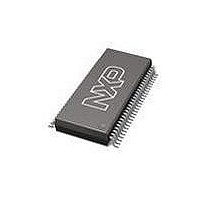
74ABT16823ADL NXP Semiconductors, 74ABT16823ADL Datasheet - Page 6

74ABT16823ADL
Manufacturer Part Number
74ABT16823ADL
Description
Flip Flops 18-BIT D-TYPE 3-S
Manufacturer
NXP Semiconductors
Datasheet
1.74ABT16823ADL.pdf
(12 pages)
Specifications of 74ABT16823ADL
Number Of Circuits
2
Logic Family
ABT
Logic Type
D-Type Edge Triggered Flip-Flop
Polarity
Non-Inverting
Input Type
Single-Ended
Propagation Delay Time
2.3 ns
High Level Output Current
- 32 mA
Supply Voltage (max)
5.5 V
Maximum Operating Temperature
+ 85 C
Mounting Style
SMD/SMT
Package / Case
SOT-371
Minimum Operating Temperature
- 40 C
Supply Voltage (min)
4.5 V
Lead Free Status / Rohs Status
Details
Other names
74ABT16823ADL,512
Available stocks
Company
Part Number
Manufacturer
Quantity
Price
1. Not more than one output should be tested at a time, and the duration of the test should not exceed one second.
2. This is the increase in supply current for each input at 3.4V.
3. For valid test results, data must not be loaded into the flip-flops (or latches) after applying the power.
4. This parameter is valid for any V
Philips Semiconductors
DC ELECTRICAL CHARACTERISTICS
NOTES:
2004 Feb 02
SYMBOL
18-bit bus-interface D-type flip-flop
with reset and enable (3-State)
I
V
transition time of up to 100 sec is permitted.
PU/PD
I
I
I
I
V
I
I
I
V
CCH
V
OFF
OZH
CEX
CCL
CCZ
OZL
RST
I
I
OH
I
OL
O
CC
IK
I
Input clamp voltage
HIGH-level output voltage
LOW-level output voltage
Power-up output LOW
voltage
Input leakage curent
Power-off leakage current
Power-up/down 3-State
output current
3-State output HIGH current V
3-State output LOW current
Output HIGH leakage
current
Output current
Quiescent supply current
Additional supply current
per input pin
PARAMETER
3
2
4
1
CC
between 0V and 2.1V with a transition time of up to 10msec. From V
V
V
V
V
V
V
V
V
V
V
V
V
V
V
V
V
V
V
V
V
other inputs at V
CC
CC
CC
CC
CC
CC
CC
CC
CC
OE
CC
CC
CC
CC
CC
I
CC
I
CC
I
CC
= GND or V
= GND or V
= GND or V
= 2.1 V; V
= 4.5 V; I
= 4.5 V; I
= 5.0 V; I
= 4.5 V; I
= 4.5 V; I
= 5.5 V; I
= 5.5 V; V
= 0.0 V; V
= Don’t care
= 5.5 V; V
= 5.5 V; V
= 5.5 V; V
= 5.5 V; V
= 5.5 V; Outputs HIGH;
= 5.5V; Outputs LOW;
= 5.5V; Outputs 3–State;
= 5.5V; one input at 3.4 V,
TEST CONDITIONS
IK
OH
OH
OH
OL
OL
O
CC
CC
CC
I
O
O
O
O
O
= V
= –18 mA
= 0.5 V; V
CC
= 64 mA; V
= 1 mA; V
or V
= 2.7 V; V
= 0.5 V; V
= 5.5 V; V
= 2.5 V
= –3 mA; V
= –3 mA; V
= –32 mA; V
CC
or GND
I
or GND
4.5 V
I
I
I
I
I
= GND or V
6
= V
= V
= GND or V
= GND or V
I
I
I
= V
= V
= V
I
= V
IL
IL
IL
IL
IL
or V
or V
IL
or V
or V
or V
or V
IH
IH
IH
IH
IH
CC
CC
CC
IH
;
MIN
–50
2.5
3.0
2.0
–
–
–
–
–
–
–
–
–
–
–
–
–
T
amb
TYP
–0.9
0.42
0.13
–1.0
–80
= +25 C
2.9
3.4
2.4
0.01
1.0
0.5
9.0
0.5
0.2
50
5.0
5.0
CC
MAX
–180
–1.2
0.55
0.55
LIMITS
–10
100
10
50
19
50
–
–
–
1
1
1
1
= 2.1V to V
74ABT16823A
T
amb
MIN
–50
2.5
3.0
2.0
–
–
–
–
–
–
–
–
–
–
–
–
–
+85 C
= –40 C to
CC
= 5V
MAX
–180
–1.2
0.55
0.55
–10
100
10
50
19
–
–
–
50
1
1
1
1
Product data
10% a
UNIT
mA
mA
mA
mA
mA
V
V
V
V
V
V
A
A
A
A
A
A


