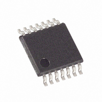
MAX4737EUD+ Maxim Integrated Products, MAX4737EUD+ Datasheet

MAX4737EUD+
Specifications of MAX4737EUD+
Related parts for MAX4737EUD+
MAX4737EUD+ Summary of contents
Page 1
... These switches are also available in a 14-pin TSSOP and a 16-pin thin QFN (4mm x 4mm) package. Battery-Operated Equipment Audio/Video-Signal Routing Low-Voltage Data-Acquisition Systems Sample-and-Hold Circuits Data-Acquisition Systems Communications Circuits UCSP is a trademark of Maxim Integrated Products, Inc. Pin Configurations/Functional Diagrams/Truth Tables MAX4737 TOP VIEW 1 2 (BUMPS SIDE DOWN) A ...
Page 2
Quad SPST Analog Switches in UCSP ABSOLUTE MAXIMUM RATINGS (All Voltages Referenced to GND) V+, IN_...................................................................-0.3V to +6.0V COM_, NO_, NC_ (Note 1) ...........................-0.3V to (V+ + 0.3V) Continuous Current COM_, NO_, NC_ ...........................±100mA Peak Current COM_, NO_, ...
Page 3
Quad SPST Analog Switches in UCSP ELECTRICAL CHARACTERISTICS—Single +3V Supply (continued) (V+ = +2.7V to +3.6V +1.4V +25°C, unless otherwise noted.) (Notes PARAMETER SYMBOL DYNAMIC CHARACTERISTICS Turn-On Time Turn-Off ...
Page 4
Quad SPST Analog Switches in UCSP ELECTRICAL CHARACTERISTICS—Single +3V Supply (continued) (V+ = +2.7V to +3.6V +1.4V +25°C, unless otherwise noted.) (Notes PARAMETER SYMBOL SUPPLY Supply Voltage Range ...
Page 5
Quad SPST Analog Switches in UCSP ELECTRICAL CHARACTERISTICS—Single +5V Supply (continued) (V+ = +4.2V to +5.5V +2.0V +25°C, unless otherwise noted.) (Notes PARAMETER SYMBOL Break-Before-Make Time Delay (MAX4739 Only) ...
Page 6
Quad SPST Analog Switches in UCSP (T = +25°C, unless otherwise noted.) A ON-RESISTANCE vs. V COM ...
Page 7
Quad SPST Analog Switches in UCSP (T = +25°C, unless otherwise noted.) A TURN-ON/OFF TIME vs. TEMPERATURE 3. 5. ...
Page 8
Quad SPST Analog Switches in UCSP (T = +25°C, unless otherwise noted.) A TOTAL HARMONIC DISTORTION vs. FREQUENCY 600Ω L 0.1 0.01 10 100 PIN MAX4738 MAX4737 THIN UCSP TSSOP UCSP TSSOP ...
Page 9
Quad SPST Analog Switches in UCSP MAX4738 MAX4737 THIN UCSP TSSOP UCSP TSSOP QFN — — — — — — ...
Page 10
Quad SPST Analog Switches in UCSP MAX4737/ V+ MAX4738/ MAX4739 V+ COM_ NO_ NC_ IN_ GND LOGIC INPUT C INCLUDES FIXTURE AND STRAY CAPACITANCE OUT COM R ...
Page 11
Quad SPST Analog Switches in UCSP TxD+ R TxD 39Ω 50pF DELAY DUE TO SWITCH FOR RISING INPUT AND RISING OUTPUT SIGNALS DELAY ...
Page 12
Quad SPST Analog Switches in UCSP MAX4737/ MAX4738/ MAX4739 R GEN NC_ OR NO_ V GEN GND IN_ Figure 4. Charge Injection 0.1µF SIGNAL V+ GENERATOR MAX4737/ 0dBm NC_ or NO_ MAX4738/ MAX4739 50Ω* COM_ ...
Page 13
Quad SPST Analog Switches in UCSP Pin Configurations/Functional Diagrams/Truth Tables (continued) TOP VIEW MAX4737 NO1 1 14 COM1 2 13 NO2 3 12 COM2 4 11 IN2 5 10 IN3 6 9 GND 7 8 TSSOP INPUT SWITCH ...
Page 14
Quad SPST Analog Switches in UCSP (The package drawing(s) in this data sheet may not reflect the most current specifications. For the latest package outline information www.maxim-ic.com/packages.) 14 ______________________________________________________________________________________ Package Information PACKAGE OUTLINE, 4x4 UCSP 1 ...
Page 15
Quad SPST Analog Switches in UCSP (The package drawing(s) in this data sheet may not reflect the most current specifications. For the latest package outline information www.maxim-ic.com/packages.) ______________________________________________________________________________________ Package Information (continued) PACKAGE OUTLINE 12, 16, 20, ...
Page 16
... Maxim cannot assume responsibility for use of any circuitry other than circuitry entirely embodied in a Maxim product. No circuit patent licenses are implied. Maxim reserves the right to change the circuitry and specifications without notice at any time. 16 ____________________Maxim Integrated Products, 120 San Gabriel Drive, Sunnyvale, CA 94086 408-737-7600 © 2004 Maxim Integrated Products ...


