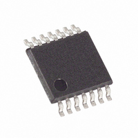
MAX4737EUD+ Maxim Integrated Products, MAX4737EUD+ Datasheet - Page 5

MAX4737EUD+
Manufacturer Part Number
MAX4737EUD+
Description
IC SWITCH QUAD SPST 14TSSOP
Manufacturer
Maxim Integrated Products
Datasheet
1.MAX4739EBET.pdf
(16 pages)
Specifications of MAX4737EUD+
Function
Switch
Circuit
4 x SPST - NO
On-state Resistance
4.5 Ohm
Voltage Supply Source
Single Supply
Voltage - Supply, Single/dual (±)
1.8 V ~ 5.5 V
Current - Supply
1µA
Operating Temperature
-40°C ~ 85°C
Mounting Type
Surface Mount
Package / Case
14-TSSOP
Number Of Switches
Quad
Switch Configuration
SPST
On Resistance (max)
5 Ohms
On Time (max)
100 ns
Off Time (max)
50 ns
Off Isolation (typ)
- 80 dB
Supply Voltage (max)
5.5 V
Supply Voltage (min)
1.8 V
Supply Current
1 uA
Maximum Power Dissipation
500 mW
Maximum Operating Temperature
+ 85 C
Mounting Style
SMD/SMT
Minimum Operating Temperature
- 40 C
Off State Leakage Current (max)
1 nA
Lead Free Status / RoHS Status
Lead free / RoHS Compliant
ELECTRICAL CHARACTERISTICS—Single +5V Supply (continued)
(V+ = +4.2V to +5.5V, V
T
Note 3:
Note 5:
Note 6:
Note 7:
Note 8:
Note 9:
Note 10: Between any two switches.
Note 4:
Break-Before-Make Time Delay
(MAX4739 Only) (Note 8)
Skew (Note 8)
DIGITAL I/O
Input Logic High Voltage
Input Logic Low Voltage
Input Leakage Current
POWER SUPPLY
Power-Supply Range
Positive Supply Current
A
= +25°C, unless otherwise noted.) (Notes 3, 4)
UCSP parts are 100% tested at +25°C only, and guaranteed by design over the specified temperature range. TSSOP and
thin QFN parts are 100% tested at T
The algebraic convention used in this data sheet is where the most negative value is a minimum and the most positive
value is a maximum.
Guaranteed by design.
Off-Isolation = 20log
Guaranteed by design for UCSP and thin QFN parts.
∆R
Flatness is defined as the difference between the maximum and minimum value of on-resistance as measured over the
specified analog signal ranges.
PARAMETER
ON
4.5 Ω Quad SPST Analog Switches in UCSP
= R
ON(MAX)
_______________________________________________________________________________________
IH
= +2.0V, V
- R
10
ON(MIN)
(V
COM
SYMBOL
t
IL
.
t
SKEW
/ V
BBM
V
V
V+
I
I+
IN
= +0.8V, T
IH
IL
NO
), V
MAX
COM
V
R
R
V+ = 5.5V, V
V+ = 5.5V, V
and guaranteed by design over the specified temperature range.
NO_
L
S
= 300Ω, C
= 39Ω, C
A
= output, V
, V
= T
NC_
MIN
CONDITIONS
= 3.0V;
L
IN
IN_
L
to T
= 50pF, Figure 3
_ = 0V or V+
= 35pF, Figure 2
NO
= 0V or V+
MAX
= input to off switch.
, unless otherwise noted. Typical values are at V+ = +5.0V,
T
T
T
T
T
T
T
+25°C
T
T
T
T
T
T
T
MIN
MIN
MIN
MIN
MIN
MIN
MIN
MAX
MAX
MAX
MAX
MAX
MAX
MAX
T
A
to
to
to
to
to
to
to
MIN
-0.1
2.0
1.8
1
TYP
0.15
8
MAX
+0.1
0.8
5.5
2
1
UNITS
µA
µA
ns
ns
V
V
V
5


