LM4916MMX National Semiconductor, LM4916MMX Datasheet
LM4916MMX
Specifications of LM4916MMX
Available stocks


Related parts for LM4916MMX

LM4916MMX Summary of contents
Page 1
... Typical Application Boomer ® registered trademark of National Semiconductor Corporation. © 2006 National Semiconductor Corporation Key Specifications n Mono-BTL output power (R = 8Ω, V ...
Page 2
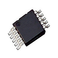
Connection Diagrams MSOP Package Top View Order Number LM4916MM See NS Package Number MUB10A for MSOP LD Package Top View Order Number LM4916LD See NS Package Number LDA10A www.national.com 20048702 Bottom Line - Part Number 20048752 2 MSOP Marking 200487F9 ...
Page 3
Typical Connections FIGURE 2. Typical Single Ended Output Configuration Circuit FIGURE 3. Typical BTL Speaker Configuration Circuit 3 20048703 20048705 www.national.com ...
Page 4
... Absolute Maximum Ratings If Military/Aerospace specified devices are required, please contact the National Semiconductor Sales Office/ Distributors for availability and specifications. Supply Voltage Storage Temperature Input Voltage Power Dissipation (Note 2) ESD Susceptibility(Note 3) ESD Susceptibility (Note 4) Junction Temperature Solder Information Small Outline Package Vapor ...
Page 5
Note 1: Absolute Maximum Ratings indicate limits beyond which damage to the device may occur. Operating Ratings indicate conditions for which the device is functional, but do not guarantee specific performance limits. Electrical Characteristics state DC and AC electrical specifications ...
Page 6
Typical Performance Characteristics THD+N vs Frequency V = 1.5V 5mW < BW 80kHz, Single Ended Output THD+N vs Frequency V = 1.2V 5mW 16Ω, Single Ended Output ...
Page 7
Typical Performance Characteristics THD+N vs Output Power V = 1.2V 16Ω 1kHz DD L Single Ended Output, A Output Power vs Supply Voltage f = 1kHz 16Ω, L Single Ended Output, A Output Power ...
Page 8
Typical Performance Characteristics Output Power vs Load Resistance V = 1.2V 1kHz DD Single Ended Output, A Power Dissipation vs Output Power < 1kHz, THD+N 1%, A Single Ended Output, Both Channels Channel Separation R = ...
Page 9
Typical Performance Characteristics Power Supply Rejection Ratio V = 1.5V 200mV DD RIPPLE R = 8Ω, BTL L Input Terminated into 10Ω Power Supply Rejection Ratio V = 1.2V 200mV DD RIPPLE R = 8Ω, BTL ...
Page 10
Typical Performance Characteristics Supply Voltage vs Supply Current Noise Floor VDD = 1.5V, Single Ended Output 16Ω, 80kHz Bandwith Shutdown Hystresis Voltage V = 1.5V DD www.national.com (Continued) 200487F1 V DD 8Ω, 80kHz Bandwith 200487B7 Power Derating Curve 200487E1 10 ...
Page 11
Typical Performance Characteristics Mute Attenuation vs Load Resistance Application Information SINGLE ENDED (SE) CONFIGURATION EXPLANATION As shown in Figure 2, the LM4916 has two operational amplifiers internally, which have externally configurable gain. The closed loop gain of the two configurable ...
Page 12
Application Information down pin of the LM4916 is also being driven by an open drain output of an external microcontroller on a separate supply. This circuit ensures that shutdown is disabled when powering up the LM4916 by either allowing shutdown ...
Page 13
Application Information FIGURE 5. Turn-On, Shutdown, and Mute Timing for Cap-Coupled Mode POWER DISSIPATION Power dissipation is a major concern when designing a successful amplifier, whether the amplifier is bridged or single-ended. A direct consequence of the increased power delivered ...
Page 14
... Further detailed and specific information concerning PCB layout, fabrication, and mounting an LD (LLP) package is available from National Semiconductor’s Package Engineer- ing Group under application note AN1187. POWER SUPPLY BYPASSING As with any amplifier, proper supply bypassing is important for low noise performance and high power supply rejection ...
Page 15
Application Information limited frequency response reap little improvement by using a high value input capacitor. In addition to system cost and size, turn on time is affected by the size of the input coupling capacitor larger input ...
Page 16
Application Information f = 100Hz/5 = 20Hz 20kHz * 5 = 100kHz H As stated in the External Components section, R junction with C creates a i www.national.com ≥ (2π * 20kΩ * 20Hz) = ...
Page 17
Revision History Rev Date 1.0 7/11/03 1.1 7/25/06 Deleted the RL labels on curves E5, E6, E3, and E4, per Allan S., then re-released the D/S to the WEB. Description Re-released the D/S to the WEB. 17 www.national.com ...
Page 18
Physical Dimensions unless otherwise noted www.national.com inches (millimeters) MSOP Package Order Number LM4916MM NS Package Number MUB10A LD Package Order Number LM4916LD NS Package Number LDA10A 18 ...
Page 19
... BANNED SUBSTANCE COMPLIANCE National Semiconductor follows the provisions of the Product Stewardship Guide for Customers (CSP-9-111C2) and Banned Substances and Materials of Interest Specification (CSP-9-111S2) for regulatory environmental compliance. Details may be found at: www.national.com/quality/green. ...