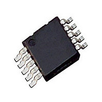
LM4916MMX National Semiconductor, LM4916MMX Datasheet - Page 13

LM4916MMX
Manufacturer Part Number
LM4916MMX
Description
Manufacturer
National Semiconductor
Datasheet
1.LM4916MMX.pdf
(19 pages)
Specifications of LM4916MMX
Operational Class
Class-AB
Audio Amplifier Output Configuration
1-Channel Mono/2-Channel Stereo
Audio Amplifier Function
Headphone/Speaker
Total Harmonic Distortion
0.1@8Ohm@25mW%
Dual Supply Voltage (typ)
Not RequiredV
Power Supply Requirement
Single
Rail/rail I/o Type
No
Power Supply Rejection Ratio
66dB
Single Supply Voltage (min)
900mV
Single Supply Voltage (max)
2.5V
Dual Supply Voltage (min)
Not RequiredV
Dual Supply Voltage (max)
Not RequiredV
Operating Temp Range
-40C to 85C
Operating Temperature Classification
Industrial
Mounting
Surface Mount
Pin Count
10
Package Type
MSOP
Lead Free Status / Rohs Status
Not Compliant
Available stocks
Company
Part Number
Manufacturer
Quantity
Price
Part Number:
LM4916MMX
Manufacturer:
NS/国半
Quantity:
20 000
Application Information
POWER DISSIPATION
Power dissipation is a major concern when designing a
successful amplifier, whether the amplifier is bridged or
single-ended. A direct consequence of the increased power
delivered to the load by a bridge amplifier is an increase in
internal power dissipation. Since the LM4916 has two opera-
tional amplifiers in one package, the maximum internal
power dissipation is 4 times that of a single-ended amplifier.
The maximum power dissipation for a given BTL application
can be derived from the power dissipation graphs or from
Equation 1.
When operating in Single Ended mode, Equation 2 states
the maximum power dissipation point for a single-ended
amplifier operating at a given supply voltage and driving a
specified output load.
Since the LM4916 has two operational amplifiers in one
package, the maximum internal power dissipation point is
twice that of the number that results from Equation 2. From
Equation 2, assuming a 1.5V power supply and a 16Ω load,
the maximum power dissipation point is 7mW per amplifier.
Thus the maximum package dissipation point is 14mW.
P
P
DMAX
DMAX
= 4*(V
= (V
FIGURE 5. Turn-On, Shutdown, and Mute Timing for Cap-Coupled Mode
DD
DD
)
)
2
2
/ (2π
/ (2π
2
R
2
R
L
(Continued)
)
L
)
(1)
(2)
13
The maximum power dissipation point obtained from either
Equations 1, 2 must not be greater than the power dissipa-
tion that results from Equation 3:
For package MUB10A, θ
the LM4916. Depending on the ambient temperature, T
the system surroundings, Equation 3 can be used to find the
maximum internal power dissipation supported by the IC
packaging. If the result of Equation 1 or 2 is greater than that
of Equation 3, then either the supply voltage must be de-
creased, the load impedance increased or T
the typical application of a 1.5V power supply, with a 16Ω
load, the maximum ambient temperature possible without
violating the maximum junction temperature is approximately
146˚C provided that device operation is around the maxi-
mum power dissipation point. Thus, for typical applications,
power dissipation is not an issue. Power dissipation is a
function of output power and thus, if typical operation is not
around the maximum power dissipation point, the ambient
temperature may be increased accordingly. Refer to the
Typical Performance Characteristics curves for power dissi-
pation information for lower output powers.
P
DMAX
= (T
JA
JMAX
= 175˚C/W. T
- T
A
) / θ
JA
JMAX
A
reduced. For
= 150˚C for
www.national.com
20048754
A
, of
(3)


