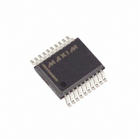
MAX4589CAP+ Maxim Integrated Products, MAX4589CAP+ Datasheet - Page 13

MAX4589CAP+
Manufacturer Part Number
MAX4589CAP+
Description
IC RF/VIDEO MUX DUAL 2CH 20-SSOP
Manufacturer
Maxim Integrated Products
Series
4000r
Datasheet
1.MAX4589EWP.pdf
(20 pages)
Specifications of MAX4589CAP+
Function
Video Multiplexer
Circuit
2 x 2:1
On-state Resistance
60 Ohm
Voltage Supply Source
Single, Dual Supply
Voltage - Supply, Single/dual (±)
2.7 V ~ 12 V, ± 2.7 V ~ 6 V
Operating Temperature
0°C ~ 70°C
Mounting Type
Surface Mount
Package / Case
20-SSOP
Lead Free Status / RoHS Status
Lead free / RoHS Compliant
The MAX4589 is constructed of high-frequency “T”
switches, as shown in Figure 8. The logic-level inputs
are translated by amplifier A1 into a V+ to V- logic sig-
nal that drives the internal control logic. The internal
control logic drives the gates of N-channel MOSFETs
N1 and N2 from V+ to V-, turning them fully on or off.
The same signal drives inverter A2 (which drives the P-
channel MOSFETs P1 and P2, turning them fully on or
off) from V+ to V-, and turns the N-channel MOSFET N3
on and off. The logic-level threshold is determined by
V
When the switch is on, MOSFETs N1, N2, P1, and P2
are on and MOSFET N3 is off (Figure 8). The signal
path is COM_ to NO_, and because both N-channel
and P-channel MOSFETs act as pure resistances, it is
symmetrical (i.e., signals pass in either direction). The
off MOSFET, N3, has no DC conduction, but has a
small amount of capacitance to GND. The MAX4589’s
construction allows an exceptional 200MHz -3dB band-
width.
Figure 7. Serial Timing Diagram
_______________Detailed Description
L
and GND.
DOUT
SCLK
DIN
CS
NOTE: ALL INPUT SIGNALS ARE SPECIFIED WITH t
TIMING IS MEASURED FROM 50% OF DIGITAL SIGNAL.
______________________________________________________________________________________
t
t
DS
CSS
Logic-Level Translators
Dual 2-Channel RF/Video Multiplexer
t
Switch On Condition
DO
t
CH
A0
t
DH
t
CL
R
AND t
A1
Low-Voltage, High-Isolation,
F
< 10ns.
Frequency response in 75Ω systems is reasonably flat
up to 50MHz, with typically 2.5dB of insertion loss.
Higher-impedance circuits show even lower attenuation
(and vice versa), but slightly lower bandwidth due to
the increased effect of the internal and external capaci-
tance and the switch’s on-resistance.
The MAX4589 is optimized for ±5V operation. Using
lower supply voltages or a single supply increases
switching time, on-resistance (and therefore on-state
attenuation), and nonlinearity.
When the switch is off, MOSFETs N1, N2, P1, and P2
are off and MOSFET N3 is on (Figure 8). The signal
path is through the parasitic off-capacitances of N1,
N2, P1, and P2, but it is shunted to ground by N3. This
forms a highpass filter whose exact characteristics are
dependent on the source and load impedances. In 75
systems, and below 1MHz, the attenuation exceeds
80dB. This value decreases with increasing frequency
and increasing circuit impedances. External capaci-
tance and board layout dominate overall performance.
BIT 3
DISABLE
t
CSH
Switch Off Condition
MAX4589
13


