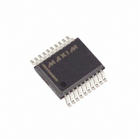
MAX4589CAP+ Maxim Integrated Products, MAX4589CAP+ Datasheet - Page 15

MAX4589CAP+
Manufacturer Part Number
MAX4589CAP+
Description
IC RF/VIDEO MUX DUAL 2CH 20-SSOP
Manufacturer
Maxim Integrated Products
Series
4000r
Datasheet
1.MAX4589EWP.pdf
(20 pages)
Specifications of MAX4589CAP+
Function
Video Multiplexer
Circuit
2 x 2:1
On-state Resistance
60 Ohm
Voltage Supply Source
Single, Dual Supply
Voltage - Supply, Single/dual (±)
2.7 V ~ 12 V, ± 2.7 V ~ 6 V
Operating Temperature
0°C ~ 70°C
Mounting Type
Surface Mount
Package / Case
20-SSOP
Lead Free Status / RoHS Status
Lead free / RoHS Compliant
The MAX4589 operates from a single supply between
+2.7V and +12V when V- is connected to GND.
Observe all of the precautions listed in the Bipolar-
Supply Operation section. Note, however, that these
parts are optimized for ±5V operation, and AC and DC
characteristics are degraded significantly when operat-
ing at less than ±5V. As the overall supply voltage
(V+ to V-) is reduced, switching speed, on-resistance,
off-isolation, and distortion are degraded (see Typical
Operating Characteristics ).
Single-supply operation also limits signal levels and
interferes with grounded signals. When V- = GND, AC
signals are limited to 300mV below GND. Voltages
below this level are clipped by the internal ESD-protec-
tion diodes, and the parts can be damaged if exces-
sive current flows.
When power to the MAX4589 is off (i.e., V+ = 0 and V-
= 0), the Absolute Maximum Ratings still apply. This
means that none of the MAX4589 pins can exceed
±0.3V. Voltages beyond ±0.3V cause the internal ESD-
protection diodes to conduct, with potentially cata-
strophic consequences.
When applying power to the MAX4589, follow this
sequence: V+, V-, V
on the analog NO_ and COM_ pins any time after V+
and V- are set. Turning on all pins simultaneously is
acceptable only if the circuit design guarantees con-
current power-up.
The power-down sequence is the opposite of the
power-up sequence. That is, the V
must go to zero potential before (or simultaneously
with) the V- then V+ supplies. Always observe the
Absolute Maximum Ratings to ensure proper operation.
Satisfactory high-frequency operation requires that
careful consideration be given to grounding. For most
applications, a ground plane is strongly recom-
mended and the GND pin must connect to it with
solid copper. While the V+ and V- power-supply pins
are common to all switches in a given package, each
input pair is separated with ground pins that are not
internally connected to each other. This contributes to
the overall high-frequency performance by reducing
channel-to-channel crosstalk.
The digital inputs have voltage thresholds determined by
V
L
and GND. (V- does not influence the logic-level
______________________________________________________________________________________
L
, then logic inputs. Apply signals
DC Ground Considerations
Power-Supply Sequencing
Dual 2-Channel RF/Video Multiplexer
Single-Supply Operation
L
and logic inputs
Grounding
Power Off
Low-Voltage, High-Isolation,
threshold.) With V
about 1.6V, ensuring compatibility with TTL- and CMOS-
logic drivers.
A ground plane is mandatory for satisfactory high-
frequency operation. Prototyping using hand wiring or
wire-wrap boards is not recommended. Make the
ground plane solid metal underneath the device, with-
out interruptions. Avoid routing traces under the device
itself. For DIP packages, this applies to both sides of a
two-sided board. Failure to observe this has a minimal
effect on the “on” characteristics of the switch at high
frequencies, but it will degrade the off-isolation and
crosstalk.
When using the SO package of the MAX4589 on PC
boards with a buried ground plane, connect the GND
pins to the ground plane with a separate via. Do not
share this via with any other ground path. Providing a
ground via on both sides of the SMT land further
enhances the off-isolation by lowering the parasitic
inductance. With the DIP package, connect the
through-holes directly to the buried plane or thermally
relieve them, as required, to meet manufacturability
requirements. Again, do not use these through-hole
pads as the current path for any other components.
Bypass the V+ and V- pins to the ground plane with sur-
face-mount 0.1µF capacitors. Locate these capacitors as
close as possible to the pins on the same side of the
board as the device. Do not use feedthroughs or vias for
bypass capacitors. If board layout dictates that the
bypass capacitors are mounted on the opposite side of
the PC board, use short feedthroughs or vias, directly
under the V+ and V- pins. Use multiple vias if possible. If
V- = GND, connect it directly to the ground plane with
solid copper. Keep all traces short.
Keep all signal traces as short as possible. Separate all
signal traces from each other, and keep them away
from any other traces that could induce interference.
Separating the signal traces with generously sized
ground wires also helps minimize interference. Routing
signals via coaxial cable, terminated as close to the
MAX4589 as possible, provides the highest isolation.
IC sockets degrade high-frequency performance and
are not recommended if signal bandwidth exceeds
5MHz. Surface-mount parts, having shorter internal
lead frames, provide the best high-frequency perfor-
mance. Keep all bypass capacitors close to the device,
and separate all signal leads with ground planes. Use
L
= +5V and GND = 0, the threshold is
AC Ground and Bypassing
Signal Routing
Board Layout
15


