DG303ACJ+ Maxim Integrated Products, DG303ACJ+ Datasheet - Page 2
DG303ACJ+
Manufacturer Part Number
DG303ACJ+
Description
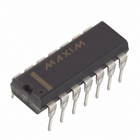
IC SWITCH DUAL SPDT 14DIP
Manufacturer
Maxim Integrated Products
Type
Analog Switchr
Datasheet
1.DG303ACWE.pdf
(11 pages)
Specifications of DG303ACJ+
Function
Switch
Circuit
2 x SPDT
On-state Resistance
50 Ohm
Voltage Supply Source
Dual Supply
Voltage - Supply, Single/dual (±)
±5 V ~ 18 V
Operating Temperature
0°C ~ 70°C
Mounting Type
Through Hole
Package / Case
14-DIP (0.300", 7.62mm)
Number Of Switches
Single
Switch Configuration
SPDT
On Resistance (max)
50 Ohms
On Time (max)
300 ns
Off Time (max)
250 ns
Off Isolation (typ)
62 dB
Supply Voltage (max)
18 V
Supply Voltage (min)
5 V
Supply Current
0.23 mA
Maximum Power Dissipation
470 mW
Maximum Operating Temperature
+ 70 C
Mounting Style
Through Hole
Minimum Operating Temperature
0 C
Off State Leakage Current (max)
0.1 nA
Package
14PDIP N
Maximum On Resistance
50@±15V Ohm
Maximum High Level Output Current
30 mA
Number Of Channels Per Chip
2
Maximum Turn-off Time
250@±15V ns
Maximum Turn-on Time
300@±15V ns
Switch Architecture
SPDT
Power Supply Type
Single|Dual
Lead Free Status / RoHS Status
Lead free / RoHS Compliant


ABSOLUTE MAXIMUM RATINGS
Voltages Referenced to V-
V+ (DG300–DG303)...............................................................36V
V+ (DG300A–DG303A) ..........................................................44V
GND .......................................................................................25V
Digital Inputs, V
Current, Any Terminal Except S or D ..................................30mA
Continuous Current, S or D .................................................30mA
Storage Temperature (A & B suffix)...................-65°C to +150°C
TTL Compatible CMOS Analog Switches
Stresses beyond those listed under “Absolute Maximum Ratings” may cause permanent damage to the device. These are stress ratings only, and functional
operation of the device at these or any other conditions beyond those indicated in the operational sections of the specifications is not implied. Exposure to
absolute maximum rating conditions for extended periods may affect device reliability.
ELECTRICAL CHARACTERISTICS
(V+ = +15V, V- = -15V, GND = 0V, T
2
(pulsed at 1ms, 10% duty cycle max) ..........................100mA
_______________________________________________________________________________________
Analog Signal Range
Drain-Source
ON-Resistance
Source OFF-
Leakage Current
Drain OFF-
Leakage Current
Drain ON-
Leakage Current
Input Current/
Voltage High
Input Current/
Voltage Low
Turn-ON Time
Turn-OFF Time
Break-Before-Make
Interval
Charge Injection
Source OFF-
Capacitance
Drain OFF-
Capacitance
Channel ON-
Capacitance
Input Capacitance
Off-Isolation (Note 4)
Crosstalk
(Channel-to-Channel)
PARAMETER
S
, V
D
, (Note 1).......................-4V to (V+ + 4V) or
(C suffix) .........................-65°C to +125°C
t
SYMBOL
V
C
ON
R
C
C
I
I
C
ANALOG
I
D(ON)
S(OFF)
D(OFF)
DS(ON)
D(ON)
S(OFF)
D(OFF)
t
I
I
t
S(ON)
C
OFF
INH
INL
ON
Q
- t
IN
30mA, whichever occurs first
OFF
A
+
= +25°C, unless otherwise noted.)
I
V
V
V
See Switching Time Test Circuit
See Break-Before-Make Time Test
Circuit, DG301(A)/DG303(A) only
C
f = 1MHz
V
V
V
V
V
V
S
f = 1MHz,
IN
IN
IN
IN
S
IN
IN
L
IN
IN
= 10mA, V
= 1V
= 10nF, R
= 5.0V
= 15V
= 0V
= 0V, R
= 0.8V
= 0.8V
= 0.8V
= 4.0V
or
or
TEST CONDITIONS
RMS
L
, f = 500kHz
IN
I
I
V
V
V
V
V
V
V
V
V
V
V
= 1kΩ
GEN
S
S
S
S
S
S
D
D
S
D
S
IN
IN
= 0.8V or 4.0V
= -10mA, V
= -10mA, V
= 14V, V
= -14V, V
= -14V, V
= 14V, V
= 0V
= VD = 0V
= V
= V
= 0V
= 0V
= 15V
= 0Ω, V
S
S
= 14V
= -14V
D
D
D
D
GEN
D
D
= -14V
= -14V
= 14V
= 14V
= 10V
= -10V
Operating Temperature (A suffix) ......................-55°C to +125°C
Lead Temperature (soldering 10s) ..................................+300°C
Power Dissipation*
Cerdip (K) (derate 11mW/°C above +75°C) ....................825mW
Plastic DIP (J) (derate 6.5mW/°C above +25°C) .............470mW
Metal Can (A) (derate 6mW/°C above +75°C).................450mW
*Device mounted with all leads soldered or welded to PC board.
= 0V
(Note 2)
MIN
DG300A–DG303AA
-15
-1
-1
-2
-1
-1
DG300–DG303A
(Note 3)
-0.001
-0.001
0.001
TYP
-0.1
-0.1
-0.1
150
130
0.1
0.1
0.1
30
30
50
12
14
14
40
74
62
6
7
(B suffix) ........................-25°C to +85°C
(C suffix) ...........................0°C to +70°C
MAX
+15
300
250
50
50
1
1
2
1
(Note 2)
DG300A–DG303AB/C
MIN
DG300–DG303B/C
-15
-5
-5
-5
-1
-1
(Note 3)
-0.001
-0.001
0.001
TYP
-0.1
-0.1
-0.1
150
130
0.1
0.1
0.1
30
30
50
12
14
14
40
62
74
6
7
MAX
+15
300
250
50
50
5
5
5
1
UNITS
pC
nA
nA
nA
µA
µA
dB
dB
ns
ns
ns
pF
pF
pF
pF
Ω
V
Related parts for DG303ACJ+
Image
Part Number
Description
Manufacturer
Datasheet
Request
R

Part Number:
Description:
MAX7528KCWPMaxim Integrated Products [CMOS Dual 8-Bit Buffered Multiplying DACs]
Manufacturer:
Maxim Integrated Products
Datasheet:
Part Number:
Description:
Single +5V, fully integrated, 1.25Gbps laser diode driver.
Manufacturer:
Maxim Integrated Products
Datasheet:
Part Number:
Description:
Single +5V, fully integrated, 155Mbps laser diode driver.
Manufacturer:
Maxim Integrated Products
Datasheet:
Part Number:
Description:
VRD11/VRD10, K8 Rev F 2/3/4-Phase PWM Controllers with Integrated Dual MOSFET Drivers
Manufacturer:
Maxim Integrated Products
Datasheet:
Part Number:
Description:
Highly Integrated Level 2 SMBus Battery Chargers
Manufacturer:
Maxim Integrated Products
Datasheet:
Part Number:
Description:
Current Monitor and Accumulator with Integrated Sense Resistor; ; Temperature Range: -40°C to +85°C
Manufacturer:
Maxim Integrated Products
Part Number:
Description:
TSSOP 14/A�/RS-485 Transceivers with Integrated 100O/120O Termination Resis
Manufacturer:
Maxim Integrated Products
Part Number:
Description:
TSSOP 14/A�/RS-485 Transceivers with Integrated 100O/120O Termination Resis
Manufacturer:
Maxim Integrated Products
Part Number:
Description:
QFN 16/A�/AC-DC and DC-DC Peak-Current-Mode Converters with Integrated Step
Manufacturer:
Maxim Integrated Products
Part Number:
Description:
TDFN/A/65V, 1A, 600KHZ, SYNCHRONOUS STEP-DOWN REGULATOR WITH INTEGRATED SWI
Manufacturer:
Maxim Integrated Products
Part Number:
Description:
Integrated Temperature Controller f
Manufacturer:
Maxim Integrated Products
Part Number:
Description:
SOT23-6/I�/45MHz to 650MHz, Integrated IF VCOs with Differential Output
Manufacturer:
Maxim Integrated Products
Part Number:
Description:
SOT23-6/I�/45MHz to 650MHz, Integrated IF VCOs with Differential Output
Manufacturer:
Maxim Integrated Products
Part Number:
Description:
EVALUATION KIT/2.4GHZ TO 2.5GHZ 802.11G/B RF TRANSCEIVER WITH INTEGRATED PA
Manufacturer:
Maxim Integrated Products
Part Number:
Description:
QFN/E/DUAL PCIE/SATA HIGH SPEED SWITCH WITH INTEGRATED BIAS RESISTOR
Manufacturer:
Maxim Integrated Products
Datasheet: