DG303ACJ+ Maxim Integrated Products, DG303ACJ+ Datasheet - Page 6
DG303ACJ+
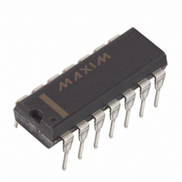
Manufacturer Part Number
DG303ACJ+
Description
IC SWITCH DUAL SPDT 14DIP
Manufacturer
Maxim Integrated Products
Type
Analog Switchr
Datasheet
1.DG303ACWE.pdf
(11 pages)
Specifications of DG303ACJ+
Function
Switch
Circuit
2 x SPDT
On-state Resistance
50 Ohm
Voltage Supply Source
Dual Supply
Voltage - Supply, Single/dual (±)
±5 V ~ 18 V
Operating Temperature
0°C ~ 70°C
Mounting Type
Through Hole
Package / Case
14-DIP (0.300", 7.62mm)
Number Of Switches
Single
Switch Configuration
SPDT
On Resistance (max)
50 Ohms
On Time (max)
300 ns
Off Time (max)
250 ns
Off Isolation (typ)
62 dB
Supply Voltage (max)
18 V
Supply Voltage (min)
5 V
Supply Current
0.23 mA
Maximum Power Dissipation
470 mW
Maximum Operating Temperature
+ 70 C
Mounting Style
Through Hole
Minimum Operating Temperature
0 C
Off State Leakage Current (max)
0.1 nA
Package
14PDIP N
Maximum On Resistance
50@±15V Ohm
Maximum High Level Output Current
30 mA
Number Of Channels Per Chip
2
Maximum Turn-off Time
250@±15V ns
Maximum Turn-on Time
300@±15V ns
Switch Architecture
SPDT
Power Supply Type
Single|Dual
Lead Free Status / RoHS Status
Lead free / RoHS Compliant


All DG300 family switches will operate with ±5V to ±15V
power supplies. They can also be used with single-ended
power supplies ranging from +10V to +30V where the V-
terminal is connected to ground. In either case, analog
signals ranging from V+ to V- can be switched.
The on-resistance variation with analog signal and supply
voltage is shown in the Typical Operating Characteristics.
The temperature coefficient of R
Typical on-resistance matching from channel to chan-
nel is 10%. In addition, Table 1 outlines some typical
parameters for single-supply operation.
TTL Compatible CMOS Analog Switches
Table 1. Typical Single Supply Parameters
6
Switching Time (R
On-Resistance
Input Logic Levels
_______________________________________________________________________________________
2.69mm
0.106"
d
c
b
e
Applications Information
L
= 1kΩ)
PARAMETER
f
a
2.74mm
0.108"
n
g
ON
m
V
V
SIGNAL
V
SIGNAL
is typically 0.5%/°C.
SIGNAL
h
t
t
OFF
ON
= V+ / 2
= +1V
= V+
i
l
k
j
0.8V, 4.0V
190ns
+10V
40ns
71Ω
77Ω
84Ω
The charge injection test circuit is shown in Figure 1.
Table 2 lists the typical injected charge for DG300 series
switches with various input voltages.
Table 2. Charge Injection (±15V Supplies)
DIE PAD
ANALOG INPUT (V)
m
b
d
g
a
c
e
h
k
n
f
i
j
l
V+ SUPPLY VOLTAGE (V- = 0V)
0.8V, 4.0V
+10
-10
+5
-5
0
150ns
+15V
40ns
51Ω
54Ω
63Ω
DG300A
DG300
GND
N.C.
N.C.
N.C.
N.C.
N.C.
IN1
IN2
D1
D2
V+
S1
S2
V-
DG301A
0.8V, 4.0V
DG301
Chip Topography
GND
N.C.
N.C.
N.C.
N.C.
N.C.
N.C.
110ns
IN1
D1
D2
V+
+20V
S1
S2
40ns
V-
42Ω
43Ω
54Ω
INJECTED Q (pC)
DG302A/DG303A
DG302/DG303
12
4
8
8
5
0.8V, 4.5V
GND
N.C.
IN1
IN2
D3
D1
D2
D4
V+
S3
S1
S2
S4
+30V
V-
70ns
40ns
31Ω
30Ω
43Ω
Related parts for DG303ACJ+
Image
Part Number
Description
Manufacturer
Datasheet
Request
R

Part Number:
Description:
MAX7528KCWPMaxim Integrated Products [CMOS Dual 8-Bit Buffered Multiplying DACs]
Manufacturer:
Maxim Integrated Products
Datasheet:
Part Number:
Description:
Single +5V, fully integrated, 1.25Gbps laser diode driver.
Manufacturer:
Maxim Integrated Products
Datasheet:
Part Number:
Description:
Single +5V, fully integrated, 155Mbps laser diode driver.
Manufacturer:
Maxim Integrated Products
Datasheet:
Part Number:
Description:
VRD11/VRD10, K8 Rev F 2/3/4-Phase PWM Controllers with Integrated Dual MOSFET Drivers
Manufacturer:
Maxim Integrated Products
Datasheet:
Part Number:
Description:
Highly Integrated Level 2 SMBus Battery Chargers
Manufacturer:
Maxim Integrated Products
Datasheet:
Part Number:
Description:
Current Monitor and Accumulator with Integrated Sense Resistor; ; Temperature Range: -40°C to +85°C
Manufacturer:
Maxim Integrated Products
Part Number:
Description:
TSSOP 14/A�/RS-485 Transceivers with Integrated 100O/120O Termination Resis
Manufacturer:
Maxim Integrated Products
Part Number:
Description:
TSSOP 14/A�/RS-485 Transceivers with Integrated 100O/120O Termination Resis
Manufacturer:
Maxim Integrated Products
Part Number:
Description:
QFN 16/A�/AC-DC and DC-DC Peak-Current-Mode Converters with Integrated Step
Manufacturer:
Maxim Integrated Products
Part Number:
Description:
TDFN/A/65V, 1A, 600KHZ, SYNCHRONOUS STEP-DOWN REGULATOR WITH INTEGRATED SWI
Manufacturer:
Maxim Integrated Products
Part Number:
Description:
Integrated Temperature Controller f
Manufacturer:
Maxim Integrated Products
Part Number:
Description:
SOT23-6/I�/45MHz to 650MHz, Integrated IF VCOs with Differential Output
Manufacturer:
Maxim Integrated Products
Part Number:
Description:
SOT23-6/I�/45MHz to 650MHz, Integrated IF VCOs with Differential Output
Manufacturer:
Maxim Integrated Products
Part Number:
Description:
EVALUATION KIT/2.4GHZ TO 2.5GHZ 802.11G/B RF TRANSCEIVER WITH INTEGRATED PA
Manufacturer:
Maxim Integrated Products
Part Number:
Description:
QFN/E/DUAL PCIE/SATA HIGH SPEED SWITCH WITH INTEGRATED BIAS RESISTOR
Manufacturer:
Maxim Integrated Products
Datasheet: