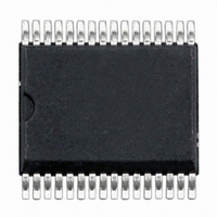
CPC5621ATR Clare, CPC5621ATR Datasheet - Page 13

CPC5621ATR
Manufacturer Part Number
CPC5621ATR
Description
IC LITELINK III FULL RING 32SOIC
Manufacturer
Clare
Series
LITELINK® IIIr
Specifications of CPC5621ATR
Function
Data Access Arrangement (DAA)
Number Of Circuits
1
Voltage - Supply
3 V ~ 5.5 V
Current - Supply
9mA
Power (watts)
1W
Operating Temperature
-40°C ~ 85°C
Mounting Type
Surface Mount
Package / Case
32-SOIC (7.5mm Width)
Includes
Caller ID Signal Reception Function, Full-Wave Ring Detection
For Use With
CLA165 - LITELINK III EVALUATION BOARDCLA164 - LITELINK III EVALUATION BOARD
Lead Free Status / RoHS Status
Lead free / RoHS Compliant
Interface
-
Other names
CLA321TR
CPC5621ATR
CPC5621ATR
Available stocks
Company
Part Number
Manufacturer
Quantity
Price
Part Number:
CPC5621ATR
Manufacturer:
LITELINK
Quantity:
20 000
3.5.1 Setting a Current Limit
LITELINK includes a telephone line current limit
feature that is selectable by choosing the desired
value for R
Clare recommends using 8.2 Ω for R
applications, limiting telephone line current to 130 mA.
Whether using the recommended value above or
when setting R
refer to the guidelines for FET thermal management
provided in AN-146,
LITELINK
3.6 AC Characteristics
3.6.1 Resistive Termination Applications
North American and Japanese telephone line AC
termination requirements are met with a resistive 600
Ω AC termination. Receive termination is applied to
the LITELINK ZNT pin (pin 29) as a 301 Ω resistor,
R
3.6.2 Reactive Termination Applications
Many countries use a single-pole complex impedance
to model the telephone network transmission line
characteristic impedance as shown in the table below.
Proper gain and termination impedance circuits for a
complex impedance requires the use of complex
network on ZNT as shown in the
Application Circuit Schematic” on page
3.6.3 Mode Pin Usage
Assert the MODE pin low to introduce a 7 dB pad into
the transmit path and add 7 dB of gain to the receive
path. These changes compensate for the gain
changes made to the transmit and receive paths in
reactive termination implementations.
R04
I
CL
ZNT
R
Amps
P
(R10).
R
S
=
C
ZDC
Designs.
P
------------ -
R
1V
ZDC
Line Impedance Model
R
R
C
ZDC
(R16) using the following formula:
S
P
P
+
0.008A
higher for a lower loop current limit
Australia
Guidelines for Effective
120 nF
220 Ω
820 Ω
100 nF
200 Ω
680 Ω
“Reactive Termination
China
8.
ZDC
for most
TBR 21
150 nF
270 Ω
750 Ω
www.clare.com
Insertion loss with MODE de-asserted and the
resistive termination application circuit is 0 dB.
Insertion loss with the reactive termination application
circuit and MODE asserted is also 0 dB.
4. Regulatory Information
LITELINK III can be used to build products that comply
with the requirements of TIA/EIA/IS-968 (formerly
FCC part 68), FCC part 15B, TBR-21, EN60950,
UL1950, EN55022B, IEC950/IEC60950, CISPR22B,
EN55024, and many other standards. LITELINK
provides supplementary isolation. Metallic surge
requirements are met through the inclusion of a
Sidactor in the application circuit. Longitudinal surge
protection is provided by LITELINK’s optical barrier
technology and the use of high-voltage components in
the application circuit as needed.
The information provided in this document is intended
to inform the equipment designer but it is not sufficient
to assure proper system design or regulatory
compliance. Since it is the equipment manufacturer's
responsibility to have their equipment properly
designed to conform to all relevant regulations,
designers using LITELINK are advised to carefully
verify that their end-product design complies with all
applicable safety, EMC, and other relevant standards
and regulations. Semiconductor components are not
rated to withstand electrical overstress or electro-static
discharges resulting from inadequate protection
measures at the board or system level.
5. LITELINK Design Resources
The Clare, Inc. web site has a wealth of information
useful for designing with LITELINK, including
application notes and reference designs that already
meet all applicable regulatory requirements. See the
following links:
LITELINK datasheets and reference designs
Application note AN-117
and Ring Detect Voltage Threshold
Application note AN-146,
LITELINK Designs
Application note AN-152
Design Conversion
Application note AN-155
Display Feature Signal Routing and Applications
Customize Caller ID Gain
LITELINK II to LITELINK III
Understanding LITELINK
Guidelines for Effective
CPC5620/CPC5621
13


