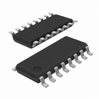
SI3018-KS Silicon Laboratories Inc, SI3018-KS Datasheet - Page 37

SI3018-KS
Manufacturer Part Number
SI3018-KS
Description
IC VOICE DAA GCI/PCM/SPI 16SOIC
Manufacturer
Silicon Laboratories Inc
Type
Chipsetr
Datasheet
1.SI3056-KS.pdf
(96 pages)
Specifications of SI3018-KS
Package / Case
16-SOIC (3.9mm Width)
Function
Data Access Arrangement (DAA)
Interface
Serial
Number Of Circuits
1
Voltage - Supply
3 V ~ 3.6 V
Current - Supply
8.5mA
Operating Temperature
0°C ~ 70°C
Mounting Type
Surface Mount
Includes
Line Voltage Monitor, Loop Current Monitor, Overload Detection, Parallel Handset Detection, Polarity Reversal Detection, TIP and
Product
Modem Chip
Supply Voltage (min)
3 V
Supply Current
8.5 mA
Maximum Operating Temperature
+ 70 C
Minimum Operating Temperature
0 C
Mounting Style
SMD/SMT
Lead Free Status / RoHS Status
Contains lead / RoHS non-compliant
Power (watts)
-
Lead Free Status / RoHS Status
Lead free / RoHS Compliant, Contains lead / RoHS non-compliant
Available stocks
Company
Part Number
Manufacturer
Quantity
Price
Company:
Part Number:
SI3018-KS
Manufacturer:
FUJITSU
Quantity:
91
Part Number:
SI3018-KS
Manufacturer:
VISHAY/威世
Quantity:
20 000
5.25.2. PLL Lock Times
The Si3056 changes sample rates quickly. However,
lock time varies based on the programming of the clock
generator. The following relationships describe the
boundaries on PLL locking time:
For
recommends
initialization. No further programming of PLL1 is
necessary. The SRC[3:0] register can be programmed
5.26. Digital Interface
The Si3056 has two serial interface modes that support
most standard modem DSPs. The M0 and M1 mode
pins select the interface mode. The key difference
between these two serial modes is the operation of the
FSYNC signal. Table 21 summarizes the serial mode
definitions.
The digital interface consists of a single, synchronous
serial link that communicates both telephony and
control data.
Mode
PLL1 lock time < 1 ms
PLL2 lock time 100 µ s to 1 ms
0
1
2
3
modem
M1 M0
0 0
0 1
1 0
1 1
MCLK
SRATE
Slave
Table 21. Serial Modes
that
FSYNC frames data
FSYNC pulse starts data frame
Slave mode
Reserved
designs,
PLL1
N1
0
Decoder
8-bit
DIV
1
be
F
UP1
Description
Silicon
programmed
M1
0
Figure 26. Update Rate of PLL1
PLL1
8-bit
DIV
Laboratories
1
98.304 MHz
during
DIV
3
Rev. 1.03
®
32.768 MHz
Decoder
for the required initial sample rate, typically 7200 Hz.
Rate changes are made by writing to SRC[3:0]
(Register 7, bits 3:0).
The final design consideration for the clock generator is
the update rate of PLL1. The following criteria must be
satisfied for the PLLs to remain stable:
where F
In serial mode 0 or 1, the Si3056 operates as a master,
where the master clock (MCLK) is an input, the serial
data clock (SCLK) is an output, and the frame sync
signal (FSYNC) is an output. The MCLK frequency and
the value of the sample rate control registers 7, 8, and 9
determine the sample rate (Fs). The serial port clock,
SCLK, runs at 256 bits per frame, where the frame rate
is equivalent to the sample rate. See "5.25.Clock
Generation" on page 36 for details on programming
sample rates.
The Si3056 transfers 16- or 15-bit telephony data in the
primary timeslot and 16-bit control data in the secondary
timeslot. Figures 27 and 28 show the relative timing of
the serial frames. Primary frames occur at the frame
rate and are always present. To minimize overhead in
the external DSP, secondary frames are present only
when requested.
Two methods exist for requesting a secondary frame to
transfer control information. The default powerup mode
uses the LSB of the 16-bit transmit (TX) data word as a
flag to request a secondary transfer. Only 15-bit TX data
is transferred, which results in a small loss of SNR but
DIV
N2
UP1
is shown in Figure 26.
F
PLL2
UP1
DIV
M2
=
F
-------------------
MCLK
N
Si3018/19/10
DIV
16
≥
144 kHz
1
0
SCLK
37


