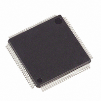
DS21554L Maxim Integrated Products, DS21554L Datasheet - Page 35

DS21554L
Manufacturer Part Number
DS21554L
Description
IC TXRX E1 1-CHIP 5V 100-LQFP
Manufacturer
Maxim Integrated Products
Datasheet
1.DS2154LNA2.pdf
(124 pages)
Specifications of DS21554L
Function
Single-Chip Transceiver
Interface
E1, HDLC, J1, T1
Number Of Circuits
1
Voltage - Supply
4.75 V ~ 5.25 V
Current - Supply
75mA
Operating Temperature
0°C ~ 70°C
Mounting Type
Surface Mount
Package / Case
100-LQFP
Includes
Remote and AIS Alarm Detector / Generator
Lead Free Status / RoHS Status
Contains lead / RoHS non-compliant
Power (watts)
-
Available stocks
Company
Part Number
Manufacturer
Quantity
Price
Part Number:
DS21554L
Manufacturer:
DALLAS
Quantity:
20 000
Company:
Part Number:
DS21554L+
Manufacturer:
Maxim
Quantity:
127
Company:
Part Number:
DS21554LB
Manufacturer:
DALLAS
Quantity:
7 214
Company:
Part Number:
DS21554LB
Manufacturer:
DALLASSEM
Quantity:
423
Company:
Part Number:
DS21554LB+
Manufacturer:
Maxim
Quantity:
90
Company:
Part Number:
DS21554LBN+
Manufacturer:
Maxim Integrated
Quantity:
10 000
TCR2: TRANSMIT CONTROL REGISTER 2 (Address = 13 Hex)
SYMBOL
(MSB)
Sa8S
AEBE
ODM
Sa8S
Sa7S
Sa6S
Sa5S
Sa4S
PF
POSITION
Sa7S
TCR2.0
TCR2.7
TCR2.6
TCR2.5
TCR2.4
TCR2.3
TCR2.2
TCR2.1
Sa6S
Sa8 Bit Select. Set to one to source the Sa8 bit from the TLINK pin; set
to zero to not source the Sa8 bit. See Section
Sa7 Bit Select. Set to one to source the Sa7 bit from the TLINK pin; set
to zero to not source the Sa7 bit. See Section
Sa6 Bit Select. Set to one to source the Sa6 bit from the TLINK pin; set
to zero to not source the Sa6 bit. See Section
Sa5 Bit Select. Set to one to source the Sa5 bit from the TLINK pin; set
to zero to not source the Sa5 bit. See Section
Sa4 Bit Select. Set to one to source the Sa4 bit from the TLINK pin; set
to zero to not source the Sa4 bit. See Section
Output Data Mode.
0 = pulses at TPOSO and TNEGO are one full TCLKO period wide
1 = pulses at TPOSO and TNEGO are 1/2 TCLKO period wide
Automatic E–Bit Enable.
0 = E–bits not automatically set in the transmit direction
1 = E–bits automatically set in the transmit direction
Function of RLOS/LOTC Pin.
0 = Receive Loss of Sync (RLOS)
1 = Loss of Transmit Clock (LOTC)
Sa5S
35 of 124
NAME AND DESCRIPTION
Sa4S
ODM
18.2
18.2
18.2
18.2
18.2
for timing details.
for timing details.
for timing details.
for timing details.
for timing details.
AEBE
(LSB)
PF


