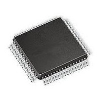
SI3220-FQ Silicon Laboratories Inc, SI3220-FQ Datasheet - Page 67

SI3220-FQ
Manufacturer Part Number
SI3220-FQ
Description
IC SLIC/CODEC DUAL-CH 64TQFP
Manufacturer
Silicon Laboratories Inc
Series
ProSLIC®r
Specifications of SI3220-FQ
Function
Subscriber Line Interface Concept (SLIC), CODEC
Interface
GCI, PCM, SPI
Number Of Circuits
2
Voltage - Supply
3.3V, 5V
Current - Supply
65mA
Power (watts)
941mW
Operating Temperature
0°C ~ 70°C
Mounting Type
Surface Mount
Package / Case
*
Includes
Battery Switching, BORSCHT Functions, DTMF Generation and Decoding, FSK Tone Generation, Modem and Fax Tone Detection
Product
Telecom
Lead Free Status / RoHS Status
Lead free / RoHS Compliant
Available stocks
Company
Part Number
Manufacturer
Quantity
Price
Company:
Part Number:
SI3220-FQ
Manufacturer:
Silicon Laboratories Inc
Quantity:
10 000
Part Number:
SI3220-FQ
Manufacturer:
N/A
Quantity:
20 000
Company:
Part Number:
SI3220-FQR
Manufacturer:
SILICON
Quantity:
12 000
are also available to allow muting of the transmit and
receive paths without requiring modifications to the
TXGAIN or RXGAIN settings.
TXEQ/RXEQ Equalizer Blocks
The TXEQ and RXEQ blocks (see Figure 11 on page
24) represent 4-tap filters that can be used to equalize
the transmit and receive paths, respectively. The
transmit path equalizer is controlled by the TXEQCO0-
TXEQCO3 RAM locations, and the receive path
equalizer is controlled by the RXEQCO0-RXEQCO3
RAM locations. The Si322x Coefficient Generator
software uses these filters in calculating the ac
impedance coefficients for optimal ac performance.
Refer to “AN63: Si322x Coefficient Generator User’s
Guide” for more detailed information regarding the
calculation of ac impedance coefficients.
Audio Characteristics
The dominant source of distortion and noise in both the
transmit and receive paths is the quantization noise
introduced by the µ -law or the A-law compression
process. Figure 5 on page 20 specifies the minimum
Signal-to-Noise and Distortion Ratio for either path for a
sine wave input of 200 Hz to 3400 Hz.
Both the µ -law and the A-law speech encoding allow the
audio codec to transfer and process audio signals larger
than 0 dBm0 without clipping. The maximum PCM code
is generated for a µ -law encoded sine wave of
3.17 dBm0 or an A-law encoded sine wave of
3.14 dBm0. The device overload clipping limits are
driven by the PCM encoding process. Figure 6 on page
21 shows the acceptable limits for the analog-to-analog
fundamental power transfer-function, which bounds the
behavior of the device.
The transmit path gain distortion versus frequency is
shown in Figure 7 on page 21. The same figure also
presents the minimum required attenuation for out-of-
band analog signals applied on the line. The presence
of a high-pass filter transfer function ensures at least
30 dB of attenuation for signals below 65 Hz. The low-
pass filter transfer function attenuates signals above
where M = {0, 1/16384, 2/16384,...32767/16384}
Figure 39. TPGA and RPGA structure
PCM
In
TPGA or RPGA
M
X
PCM
Out
Rev. 1.0
3.4 kHz. It is implemented as part of the A-to-D
converter.
The receive path transfer function requirement, shown
in Figure 8 on page 22, is very similar to the transmit
path transfer function. The PCM data rate is 8 kHz; so,
no frequencies greater than 4 kHz are digitally-encoded
in the data stream. At frequencies greater than 4 kHz,
the plot in Figure 8 is interpreted as the maximum
allowable magnitude of spurious signals that are
generated when a PCM data stream representing a sine
wave signal in the range of 300 Hz to 3.4 kHz at a level
of 0 dBm0 is applied at the digital input.
The group delay distortion in either path is limited to no
more than the levels indicated in Figure 9 on page 23.
The reference in Figure 9 is the smallest group delay for
a sine wave in the range of 500 Hz to 2500 Hz at
0 dBm0.
The block diagram for the voice-band signal processing
paths is shown in Figure 11 on page 24. Both the
receive and the transmit paths employ the optimal
combination of analog and digital signal processing for
maximum performance while maintaining sufficient
flexibility for users to optimize their particular application
of the device. The two-wire (TIP/RING) voice-band
interface to the device is implemented with a small
number of external components. The receive path
interface consists of a unity-gain current buffer, I
while the transmit path interface is an ac coupling
capacitor.
differentially, are shown as single-ended for simplicity.
System Clock Generation
The Dual ProSLIC devices generate the internal clock
frequencies from the PCLK input. PCLK must be
synchronous to the 8 kHz FSYNC clock and run at one
of the following rates: 256 kHz, 512 kHz, 786 kHz,
1.024 MHz,
4.096 MHz, or 8.192 MHz. The ratio of the PCLK rate to
the FSYNC rate is determined by a counter clocked by
PCLK. The three-bit ratio information is transferred into
an internal register, PLL_MULT, after a device reset.
The PLL_MULT controls the internal PLL, which
multiplies PCLK to generate the rate required to run the
internal filters and other circuitry.
The PLL clock synthesizer settles quickly after power-
up or update of the PLL-MULT register. The PLL lock
process begins immediately after the RESET pin is
pulled high and takes approximately 5 ms to achieve
lock after RESET is released with stable PCLK and
FSYNC. However, the settling time depends on the
PCLK frequency and can be predicted based on the
following equation:
Signal
1.536 MHz,
paths,
Si3220/Si3225
1.544 MHz,
although
implemented
2.048 MHz,
BUF
67
,


