PC16550DN/NOPB National Semiconductor, PC16550DN/NOPB Datasheet - Page 12
PC16550DN/NOPB
Manufacturer Part Number
PC16550DN/NOPB
Description
IC UART WITH FIFO 40-DIP
Manufacturer
National Semiconductor
Datasheet
1.PC16550DVNOPB.pdf
(22 pages)
Specifications of PC16550DN/NOPB
Features
Modem Control Function
Number Of Channels
1, UART
Fifo's
16 Byte
Voltage - Supply
4.5 V ~ 5.5 V
With False Start Bit Detection
Yes
With Modem Control
Yes
Mounting Type
Through Hole
Package / Case
40-DIP (0.600", 15.24mm)
Supply Voltage (max)
5.5 V
Supply Voltage (min)
4.5 V
Msl
MSL 1 - Unlimited
Data Rate Max
128Kbps
Ic Function
UART IC
Interface Type
Serial
No. Of Transceivers
1
Peak Reflow Compatible (260 C)
Yes
Supply Current
15mA
Rohs Compliant
Yes
Lead Free Status / RoHS Status
Lead free / RoHS Compliant
Other names
*PC16550DN
*PC16550DN/NOPB
PC16550DN
*PC16550DN/NOPB
PC16550DN
Available stocks
Company
Part Number
Manufacturer
Quantity
Price
Company:

Part Number:
PC16550DN/NOPB
Manufacturer:
NSC
Quantity:
1 011
Company:
Part Number:
PC16550DN/NOPB
Manufacturer:
National
Quantity:
695
Part Number:
PC16550DN/NOPB
Manufacturer:
TI/德州仪器
Quantity:
20 000


6 0 Pin Descriptions
OUT 2 Output 2 Pin 31 This user-designated output that
can be set to an active low by programming bit 3 (OUT 2) of
the MODEM Control Register to a high level A Master Re-
set operation sets this signal to its inactive (high) state
Loop mode operation holds this signal in its inactive state In
the XMOS parts this will achieve TTL levels
RCLK Receiver Clock Pin 9 This input is the 16
rate clock for the receiver section of the chip
RD RD Read Pins 22 and 21 When RD is high or RD is
low while the chip is selected the CPU can read status
information or data from the selected UART register
Note Only an active RD or RD input is required to transfer data from the
RI Ring Indicator Pin 39 When low this indicates that a
telephone ringing signal has been received by the MODEM
or data set The RI signal is a MODEM status input whose
condition can be tested by the CPU reading bit 6 (RI) of the
MODEM Status Register Bit 6 is the complement of the RI
signal Bit 2 (TERI) of the MODEM Status Register indicates
whether the RI input signal has changed from a low to a
high state since the previous reading of the MODEM Status
Register
Note Whenever the RI bit of the MODEM Status Register changes from a
RTS Request to Send Pin 32 When low this informs the
MODEM or data set that the UART is ready to exchange
data The RTS output signal can be set to an active low by
programming bit 1 (RTS) of the MODEM Control Register A
Master Reset operation sets this signal to its inactive (high)
state Loop mode operation holds this signal in its inactive
state
SIN Serial Input Pin 10 Serial data input from the commu-
nications link (peripheral device MODEM or data set)
SOUT Serial Output Pin 11 Composite serial data output
to the communications link (peripheral MODEM or data
set) The SOUT signal is set to the Marking (logic 1) state
upon a Master Reset operation
TXRDY RXRDY Pins 24 29 Transmitter and Receiver
DMA signalling is available through two pins (24 and 29)
When operating in the FIFO mode one of two types of DMA
signalling per pin can be selected via FCR3 When operat-
ing as in the 16450 Mode only DMA mode 0 is allowed
Mode 0 supports single transfer DMA where a transfer is
made between CPU bus cycles Mode 1 supports multi-
transfer DMA where multiple transfers are made continu-
ously until the RCVR FIFO has been emptied or the XMIT
FIFO has been filled
RXRDY Mode 0 When in the 16450 Mode (FCR0
the FIFO Mode (FCR0
character in the RCVR FIFO or RCVR holding register the
RXRDY pin (29) will be low active Once it is activated the
RXRDY pin will go inactive when there are no more charac-
ters in the FIFO or holding register
RXRDY Mode 1 In the FIFO Mode (FCR0
FCR3
reached the RXRDY pin will go low active Once it is acti-
vated it will go inactive when there are no more characters
in the FIFO or holding register
UART during a read operation Therefore tie either the RD input per-
manently low or the RD input permanently high when it is not used
high to a low state an interrupt is generated if the MODEM Status
Interrupt is enabled
e
1 and the trigger level or the timeout has been
e
1 FCR3
e
(Continued)
0) and there is at least 1
e
1) when the
e
c
0) or in
baud
12
TXRDY Mode 0 In the 16450 Mode (FCR0
FIFO Mode (FCR0
ters in the XMIT FIFO or XMIT holding register the TXRDY
pin (24) will be low active Once it is activated the TXRDY
pin will go inactive after the first character is loaded into the
XMIT FIFO or holding register
TXRDY Mode 1 In the FIFO Mode (FCR0
FCR3
TXRDY pin will go low active This pin will become inactive
when the XMIT FIFO is completely full
V
V
WR WR Write Pins 19 and 18 When WR is high or WR is
low while the chip is selected the CPU can write control
words or data into the selected UART register
Note Only an active WR or WR input is required to transfer data to the
XIN (External Crystal Input) Pin 16 This signal input is used
in conjunction with XOUT to form a feedback circuit for the
baud rate generator’s oscillator If a clock signal will be gen-
erated off-chip then it should drive the baud rate generator
through this pin
XOUT (External Crystal Output) Pin 17 This signal output is
used in conjunction with XIN to form a feedback circuit for
the baud rate generator’s oscillator If the clock signal will
be generated off-chip then this pin is unused
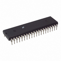
7 0 Connection Diagrams
DD
SS
UART during a write operation Therefore tie either the WR input
permanently low or the WR input permanently high when it is not
used
Pin 20 Ground (0V) reference
Pin 40
e
1 and there are no characters in the XMIT FIFO the
a
See NS Package Number N40A
5V supply
Order Number PC16550DN
e
Dual-In-Line Package
1 FCR3
Top View
e
0) and there are no charac-
e
0) or in the
e
TL C 8652 – 17
1) when
Related parts for PC16550DN/NOPB
Image
Part Number
Description
Manufacturer
Datasheet
Request
R

Part Number:
Description:
UART IC
Manufacturer:
National Semiconductor
Datasheet:

Part Number:
Description:
National Semiconductor [8-Bit D/A Converter]
Manufacturer:
National Semiconductor
Datasheet:
Part Number:
Description:
National Semiconductor [Media Coprocessor]
Manufacturer:
National Semiconductor
Datasheet:
Part Number:
Description:
Digitally Controlled Tone and Volume Circuit with Stereo Audio Power Amplifier, Microphone Preamp Stage and National 3D Sound
Manufacturer:
National Semiconductor
Datasheet:
Part Number:
Description:
Digitally Controlled Tone and Volume Circuit with Stereo Audio Power Amplifier, Microphone Preamp Stage and National 3D Sound
Manufacturer:
National Semiconductor
Datasheet:
Part Number:
Description:
AC97 Rev 2 Codec with Sample Rate Conversion and National 3D Sound
Manufacturer:
National Semiconductor
Part Number:
Description:
Manufacturer:
National Semiconductor
Datasheet:
Part Number:
Description:
Manufacturer:
National Semiconductor
Datasheet:
Part Number:
Description:
General Purpose, Low Voltage, Low Power, Rail-to-Rail Output Operational Amplifiers
Manufacturer:
National Semiconductor
Datasheet:
Part Number:
Description:
8-bit 20 MSPS flash A/D converter.
Manufacturer:
National Semiconductor
Datasheet:
Part Number:
Description:
Low Noise Quad Operational Amplifier
Manufacturer:
National Semiconductor
Datasheet:
Part Number:
Description:
Quad Differential Line Receivers
Manufacturer:
National Semiconductor
Datasheet:
Part Number:
Description:
Quad High Speed Trapezoidal? Bus Transceiver
Manufacturer:
National Semiconductor
Datasheet:
Part Number:
Description:
Dual Line Receiver
Manufacturer:
National Semiconductor
Datasheet: