PC16550DN/NOPB National Semiconductor, PC16550DN/NOPB Datasheet - Page 17
PC16550DN/NOPB
Manufacturer Part Number
PC16550DN/NOPB
Description
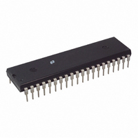
IC UART WITH FIFO 40-DIP
Manufacturer
National Semiconductor
Datasheet
1.PC16550DVNOPB.pdf
(22 pages)
Specifications of PC16550DN/NOPB
Features
Modem Control Function
Number Of Channels
1, UART
Fifo's
16 Byte
Voltage - Supply
4.5 V ~ 5.5 V
With False Start Bit Detection
Yes
With Modem Control
Yes
Mounting Type
Through Hole
Package / Case
40-DIP (0.600", 15.24mm)
Supply Voltage (max)
5.5 V
Supply Voltage (min)
4.5 V
Msl
MSL 1 - Unlimited
Data Rate Max
128Kbps
Ic Function
UART IC
Interface Type
Serial
No. Of Transceivers
1
Peak Reflow Compatible (260 C)
Yes
Supply Current
15mA
Rohs Compliant
Yes
Lead Free Status / RoHS Status
Lead free / RoHS Compliant
Other names
*PC16550DN
*PC16550DN/NOPB
PC16550DN
*PC16550DN/NOPB
PC16550DN
Available stocks
Company
Part Number
Manufacturer
Quantity
Price
Company:

Part Number:
PC16550DN/NOPB
Manufacturer:
NSC
Quantity:
1 011
Company:
Part Number:
PC16550DN/NOPB
Manufacturer:
National
Quantity:
695
Part Number:
PC16550DN/NOPB
Manufacturer:
TI/德州仪器
Quantity:
20 000


Mode
FIFO
Bit 3 Bit 2 Bit 1 Bit 0
Only
8 0 Registers
0
0
0
1
0
0
Bit 5 This bit is the Transmitter Holding Register Empty
(THRE) indicator Bit 5 indicates that the UART is ready to
accept a new character for transmission In addition this bit
causes the UART to issue an interrupt to the CPU when the
Transmit Holding Register Empty Interrupt enable is set
high The THRE bit is set to a logic 1 when a character is
transferred from the Transmitter Holding Register into the
Transmitter Shift Register The bit is reset to logic 0 concur-
rently with the loading of the Transmitter Holding Register
by the CPU In the FIFO mode this bit is set when the XMIT
FIFO is empty it is cleared when at least 1 byte is written to
the XMIT FIFO
Bit 6 This bit is the Transmitter Empty (TEMT) indicator Bit
6 is set to a logic 1 whenever the Transmitter Holding Regis-
ter (THR) and the Transmitter Shift Register (TSR) are both
empty It is reset to a logic 0 whenever either the THR or
TSR contains a data character In the FIFO mode this bit is
set to one whenever the transmitter FIFO and shift register
are both empty
Bit 7 In the 16450 Mode this is a 0 In the FIFO mode LSR7
is set when there is at least one parity error framing error or
break indication in the FIFO LSR7 is cleared when the CPU
reads the LSR if there are no subsequent errors in the
FIFO
Note The Line Status Register is intended for read operations only Writing
8 5 FIFO CONTROL REGISTER
This is a write only register at the same location as the IIR
(the IIR is a read only register) This register is used to en-
able the FIFOs clear the FIFOs set the RCVR FIFO trigger
level and select the type of DMA signalling
Bit 0 Writing a 1 to FCR0 enables both the XMIT and RCVR
FIFOs Resetting FCR0 will clear all bytes in both FIFOs
to this register is not recommended as this operation is only used for
factory testing In the FIFO mode the software must load a data byte
in the Rx FIFO via Loopback Mode in order to write to LSR2–LSR4
LSR0 and LSR7 can’t be written to in FIFO mode
0
1
1
1
0
0
Identification
Interrupt
Register
0
1
0
0
1
0
1
0
0
0
0
0
Priority
Second Received Data Available Receiver Data Available or Trigger
Second Character Timeout
Highest Receiver Line Status
(Continued)
Fourth
Level
Third
None
Indication
Transmitter Holding
Register Empty
MODEM Status
Interrupt Type
TABLE IV Interrupt Control Functions
Interrupt Set and Reset Functions
None
Overrun Error or Parity Error or
Framing Error or Break Interrupt
Level Reached
No Characters Have Been
Removed From or Input to the
RCVR FIFO During the Last 4 Char
Times and There Is at Least 1 Char
in It During This Time
Transmitter Holding
Register Empty
Clear to Send or Data Set Ready or
Ring Indicator or Data Carrier
Detect
17
When changing from the FIFO Mode to the 16450 Mode
and vice versa data is automatically cleared from the
FIFOs This bit must be a 1 when other FCR bits are written
to or they will not be programmed
Bit 1 Writing a 1 to FCR1 clears all bytes in the RCVR FIFO
and resets its counter logic to 0 The shift register is not
cleared The 1 that is written to this bit position is self-clear-
ing
Bit 2 Writing a 1 to FCR2 clears all bytes in the XMIT FIFO
and resets its counter logic to 0 The shift register is not
cleared The 1 that is written to this bit position is self-clear-
ing
Bit 3 Setting FCR3 to a 1 will cause the RXRDY and
TXRDY pins to change from mode 0 to mode 1 if FCR0
(see description of RXRDY and TXRDY pins)
Bit 4 5 FCR4 to FCR5 are reserved for future use
Bit 6 7 FCR6 and FCR7 are used to set the trigger level for
the RCVR FIFO interrupt
8 6 INTERRUPT IDENTIFICATION REGISTER
In order to provide minimum software overhead during data
character transfers the UART prioritizes interrupts into four
levels and records these in the interrupt Identification Regis-
ter The four levels of interrupt conditions in order of priority
are Receiver Line Status Received Data Ready Transmit-
ter Holding Register Empty and MODEM Status
Interrupt Source
7
0
0
1
1
6
0
1
0
1
Register or the FIFO Drops
Below the Trigger Level
Buffer Register
Reading the IIR Register (if
source of interrupt) or Writing
into the Transmitter Holding
Register
Status Register
Reading the Line Status
Register
Reading the Receiver Buffer
Reading the Receiver
Reading the MODEM
Trigger Level (Bytes)
Interrupt Reset Control
RCVR FIFO
01
04
08
14
e
1
Related parts for PC16550DN/NOPB
Image
Part Number
Description
Manufacturer
Datasheet
Request
R

Part Number:
Description:
UART IC
Manufacturer:
National Semiconductor
Datasheet:

Part Number:
Description:
National Semiconductor [8-Bit D/A Converter]
Manufacturer:
National Semiconductor
Datasheet:
Part Number:
Description:
National Semiconductor [Media Coprocessor]
Manufacturer:
National Semiconductor
Datasheet:
Part Number:
Description:
Digitally Controlled Tone and Volume Circuit with Stereo Audio Power Amplifier, Microphone Preamp Stage and National 3D Sound
Manufacturer:
National Semiconductor
Datasheet:
Part Number:
Description:
Digitally Controlled Tone and Volume Circuit with Stereo Audio Power Amplifier, Microphone Preamp Stage and National 3D Sound
Manufacturer:
National Semiconductor
Datasheet:
Part Number:
Description:
AC97 Rev 2 Codec with Sample Rate Conversion and National 3D Sound
Manufacturer:
National Semiconductor
Part Number:
Description:
Manufacturer:
National Semiconductor
Datasheet:
Part Number:
Description:
Manufacturer:
National Semiconductor
Datasheet:
Part Number:
Description:
General Purpose, Low Voltage, Low Power, Rail-to-Rail Output Operational Amplifiers
Manufacturer:
National Semiconductor
Datasheet:
Part Number:
Description:
8-bit 20 MSPS flash A/D converter.
Manufacturer:
National Semiconductor
Datasheet:
Part Number:
Description:
Low Noise Quad Operational Amplifier
Manufacturer:
National Semiconductor
Datasheet:
Part Number:
Description:
Quad Differential Line Receivers
Manufacturer:
National Semiconductor
Datasheet:
Part Number:
Description:
Quad High Speed Trapezoidal? Bus Transceiver
Manufacturer:
National Semiconductor
Datasheet:
Part Number:
Description:
Dual Line Receiver
Manufacturer:
National Semiconductor
Datasheet: