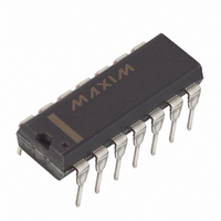
MAX3100CPD+ Maxim Integrated Products, MAX3100CPD+ Datasheet - Page 8

MAX3100CPD+
Manufacturer Part Number
MAX3100CPD+
Description
IC UART SPI MICROCOMPATBL 14-DIP
Manufacturer
Maxim Integrated Products
Type
SPI/MICROWIRE-Compatible UARTr
Datasheet
1.MAX3100CEE.pdf
(24 pages)
Specifications of MAX3100CPD+
Features
Low Power
Number Of Channels
1, UART
Fifo's
8 Byte
Protocol
RS232, RS485
Voltage - Supply
2.7 V ~ 5.5 V
With Irda Encoder/decoder
Yes
With False Start Bit Detection
Yes
With Cmos
Yes
Mounting Type
Through Hole
Package / Case
14-DIP (0.300", 7.62mm)
Data Rate
115.2 Kbps
Supply Voltage (max)
5.5 V
Supply Voltage (min)
2.7 V
Supply Current
0.27 mA
Maximum Operating Temperature
+ 70 C
Minimum Operating Temperature
0 C
Description/function
SPI/MICROWIRE-compatible UART
Mounting Style
Through Hole
Operating Supply Voltage
2.7 V to 5.5 V
Lead Free Status / RoHS Status
Lead free / RoHS Compliant
Table 1 shows write-configuration data. A 16-bit
SPI/MICROWIRE write configuration clears the receive
FIFO and the R, T, RA/FE, D0r–D7r, D0t–D7t, Pr, and Pt
registers. RTS and CTS remain unchanged. The new
configuration is valid on CS’s rising edge if the transmit
buffer is empty (T = 1) and transmission is over. If the
latest transmission has not been completed, the regis-
ters are updated when the transmission is over (T = 0).
The write-configuration bits (FEN, SHDNi, IR, ST, PE, L,
B3–B0) take effect after the current transmission is
over. The mask bits (TM, RM, PM, RAM) take effect
immediately after the 16th clock’s rising edge at SCLK.
Table 2 shows read-configuration data. This register
reads back the last configuration written to the
Table 3. Write Data (D15, D14 = 1, 0)
SPI/MICROWIRE-Compatible
UART in QSOP-16
Table 1. Write Configuration (D15, D14 = 1, 1)
Table 2. Read Configuration (D15, D14 = 0, 1)
Table 4. Read Data (D15, D14 = 0, 0)
8
DOUT
DOUT
DOUT
DOUT
DIN
DIN
DIN
DIN
BIT
BIT
BIT
BIT
_______________________________________________________________________________________
15
15
15
15
R
R
R
R
0
1
0
1
14
14
14
14
1
T
0
T
0
T
1
T
FEN
FEN
13
13
13
13
0
0
0
0
0
0
MAX3100 Operations
SHDNo
SHDNi
12
12
0
0
0
0
12
12
0
0
11
11
0
0
0
0
Write Operations
Read Operations
TM
TM
11
11
0
0
RA/FE
RA/FE
TE
10
10
0
RM
RM
10
10
0
0
CTS
CTS
RTS
PM
PM
9
0
9
9
0
9
0
RAM
RAM
Pr
Pr
Pt
8
0
8
8
0
8
0
MAX3100. The device enters test mode if bit 0 = 1. In
this mode, if CS = 0, the RTS pin acts as the 16x clock
generator’s output. This may be useful for direct baud-
rate generation (in this mode, TX and RX are in digital
loopback).
Normally, the write-data register loads the TX-buffer
register. To change the RTS pin’s state without writing
data, set the TE bit. Setting the TE bit high inhibits the
write command (Table 3).
Reading data clears the R bit and interrupt IRQ (Table 4).
Table 5 shows read/write operation and power-on reset
state (POR), and describes each bit used in program-
ming the MAX3100. Figure 5 shows parity and word-
length control.
D7t
D7r
D7r
IR
7
0
7
7
0
IR
7
0
D6t
D6r
D6r
ST
6
0
6
6
0
ST
6
0
D5t
D5r
D5r
PE
5
0
5
5
0
PE
5
0
D4t
D4r
D4r
4
0
L
4
4
0
4
L
0
D3r
D3r
D3t
B3
Register Functions
3
0
3
3
0
B3
3
0
D2r
D2r
D2t
B2
2
0
2
2
0
B2
2
0
D1r
D1r
D1t
B1
B1
1
0
1
1
0
1
0
TEST
D0t
D0r
D0r
B0
B0
0
0
0
0
0
0


