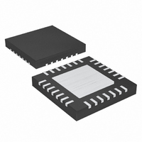
MAX9791AETI+T Maxim Integrated Products, MAX9791AETI+T Datasheet - Page 26

MAX9791AETI+T
Manufacturer Part Number
MAX9791AETI+T
Description
IC AMP AUDIO 2.2W STER D 28TQFN
Manufacturer
Maxim Integrated Products
Series
DirectDrive™r
Type
Class Dr
Datasheet
1.MAX9791AETI.pdf
(34 pages)
Specifications of MAX9791AETI+T
Output Type
2-Channel (Stereo) with Stereo Headphones and Subwoofer
Max Output Power X Channels @ Load
2.2W x 2 @ 4 Ohm; 180mW x 2 @ 32 Ohm
Voltage - Supply
4.5 V ~ 5.5 V
Features
Depop, LDO, Short-Circuit and Thermal Protection, Shutdown
Mounting Type
Surface Mount
Package / Case
28-TQFN Exposed Pad
Lead Free Status / RoHS Status
Lead free / RoHS Compliant
Windows Vista-Compliant Class D Speaker
Amplifiers with DirectDrive Headphone Amplifiers
Connect a 1µF capacitor between CPVSS and PGND.
Connect 2 x 1µF capacitors between LDO_OUT and
GND for 4.75V and 3.3V LDO options (MAX979_A and
MAX979_B, respectively). Connect two parallel 2µF
capacitors between LDO_OUT and GND for the 1.8V
LDO option (MAX979_C).
Proper layout and grounding are essential for optimum
performance. Use large traces for the power-supply
inputs and amplifier outputs to minimize losses due to
parasitic trace resistance, as well as route heat away
from the device. Good grounding improves audio per-
formance, minimizes crosstalk between channels, and
prevents switching noise from coupling into the audio
signal. Connect PGND and GND together at a single
point on the PCB. Route PGND and all traces that carry
switching transients away from GND, and the traces
and components in the audio signal path.
Connect C2 to the PGND plane. Place the charge-
pump capacitors (C1, C2) as close as possible to the
device. Bypass PVDD with a 0.1µF capacitor to PGND.
Place the bypass capacitors as close as possible to the
device.
26
______________________________________________________________________________________
Charge-Pump Output Capacitor (C2)
LDO Output Capacitor (CLDO)
Layout and Grounding
The MAX9791/MAX9792 is inherently designed for
excellent RF immunity. For best performance, add
ground fills around all signal traces on top or bottom
PCB planes.
Use large, low-resistance output traces. As load imped-
ance decreases, the current drawn from the device out-
puts increase. At higher current, the resistance of the
output traces decrease the power delivered to the load.
For example, if 2W is delivered from the speaker output
to a 4Ω load through a 100mΩ trace, 49mW is wasted
in the trace. If power is delivered through a 10mΩ
trace, only 5mW is wasted in the trace. Large output,
supply, and GND traces also improve the power dissi-
pation of the device.
The MAX9791/MAX9792 thin QFN package features an
exposed thermal pad on its underside. This pad lowers
the package’s thermal resistance by providing a direct
heat conduction path from the die to the printed circuit
board. Connect the exposed thermal pad to GND by
using a large pad and multiple vias to the GND plane.
PROCESS: BiCMOS
Chip Information


