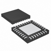
MAX9765ETJ+ Maxim Integrated Products, MAX9765ETJ+ Datasheet - Page 18

MAX9765ETJ+
Manufacturer Part Number
MAX9765ETJ+
Description
IC AMP AUDIO .75W STER AB 32TQFN
Manufacturer
Maxim Integrated Products
Type
Class ABr
Datasheet
1.MAX9766ETJ.pdf
(33 pages)
Specifications of MAX9765ETJ+
Output Type
2-Channel (Stereo) with Stereo Headphones
Max Output Power X Channels @ Load
750mW x 2 @ 4 Ohm; 65mW x 2 @ 16 Ohm
Voltage - Supply
2.7 V ~ 5.5 V
Features
Depop, I²C, Input Multiplexer, Microphone, Mute, Short-Circuit and Thermal Protection, Shutdown
Mounting Type
Surface Mount
Package / Case
32-TQFN Exposed Pad
Lead Free Status / RoHS Status
Lead free / RoHS Compliant
750mW Audio Amplifiers with Headphone Amp,
Microphone Preamp, and Input Mux
mode, this waveform shapes the frequency spectrum,
minimizing the amount of audible components present
at the headphone. In speaker mode, the BTL amplifiers
start up in the same fashion as in headphone mode.
When entering shutdown, both amplifier outputs ramp
to GND quickly and simultaneously. The devices can
also be connected to a standby power source that
ensures that the device undergoes its full shutdown
cycle even after power has been removed. The value of
the capacitor on the BIAS pin affects the click-and-pop
energy. For optimum click/pop performance, use a 1µF
capacitor.
The MAX9765/MAX9766/MAX9767 feature a system
that provides clickless power-down when power is
removed from the device. SV
ondary supply that powers the device through its shut-
down cycle when V
the amplifier output DC level slowly ramps to GND,
ensuring clickless power-down. If clickless power-down
is required, connect SV
supply that is always on, or connect a reservoir capaci-
tor from SV
nected to either a secondary power supply or reservoir
capacitor for normal device operation. If click-and-pop
suppression during power-down is not required, con-
nect SV
The clickless power-down cycle only occurs when the
device is in headphone mode. The speaker mode is
inherently clickless, the differential architecture cancels
the DC shift across the speaker. The MAX9765/
MAX9766/MAX9767 BTL outputs are pulled to GND
quickly and simultaneously, resulting in no audible
components. If the MAX9765/MAX9766/MAX9767 are
only used as speaker amplifiers, then reservoir capaci-
tors or secondary supplies are not necessary.
When using a reservoir capacitor, a 220µF capacitor
provides optimum charge storage for the shutdown
cycle for all conditions. If a smaller reservoir capacitor
is desired, decrease the size of C
causes the output DC level to decay at a faster rate,
increasing the audible content at the speaker, but
reducing the duration of the shutdown cycle.
The MAX9765/MAX9766 feature an I
ible 2-wire serial interface consisting of a serial data
line (SDA) and a serial clock line (SCL). SDA and SCL
facilitate bidirectional communication between the
MAX9765/MAX9766 and the master at clock rates up to
400kHz. Figure 3 shows the 2-wire interface timing dia-
gram. The MAX9765/MAX9766 are transmit/receive
18
______________________________________________________________________________________
DD
to V
DD
to GND. SV
DD
directly.
DD
Standby Power Supply (SV
DD
is removed. During this cycle,
DD
to either a secondary power
does not need to be con-
DD
BIAS
Digital Interface
is an optional sec-
2
C/SMBus-compat-
. A smaller C
BIAS
DD
)
slave-only devices, relying upon a master to generate a
clock signal. The master (typically a microcontroller) ini-
tiates data transfer on the bus and generates SCL to
permit that transfer.
A master device communicates to the MAX9765/
MAX9766 by transmitting the proper address followed
by a command and/or data words. Each transmit
sequence is framed by a START (S) or REPEATED
START (S
word transmitted over the bus is 8 bits long and is
always followed by an acknowledge clock pulse.
The MAX9765/MAX9766 SDA and SCL amplifiers are
open-drain outputs requiring a pullup resistor to gener-
ate a logic-high voltage. Series resistors in line with
SDA and SCL are optional. These series resistors pro-
tect the input stages of the devices from high-voltage
spikes on the bus lines, and minimize crosstalk and
undershoot of the bus signals.
One data bit is transferred during each SCL clock
cycle. The data on SDA must remain stable during the
high period of the SCL clock pulse. Changes in SDA
while SCL is high are control signals (see the START
and STOP Conditions section). SDA and SCL idle high
when the I
When the serial interface is inactive, SDA and SCL idle
high. A master device initiates communication by issu-
ing a START condition. A START condition is a high-to-
low transition on SDA with SCL high. A STOP condition
is a low-to-high transition on SDA while SCL is high
(Figure 4). A START condition from the master signals
the beginning of a transmission to the MAX9765/
MAX9766. The master terminates transmission by issu-
ing the STOP condition; this frees the bus. If a REPEAT-
ED START condition is generated instead of a STOP
Figure 2. HPS Configuration Circuit
r
2
MAX9765
MAX9766
) condition and a STOP (P) condition. Each
C bus is not busy.
OUTR+
OUTL+
HPS
10kΩ
START and STOP Conditions
47kΩ
R2
R3
10kΩ
3V
R1
680kΩ
Bit Transfer


