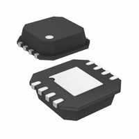
AD8337BCPZ-WP Analog Devices Inc, AD8337BCPZ-WP Datasheet - Page 21

AD8337BCPZ-WP
Manufacturer Part Number
AD8337BCPZ-WP
Description
IC AMP VGA DC-COUPLED GP 8-LFCSP
Manufacturer
Analog Devices Inc
Series
X-AMP®r
Type
Variable Gain Amplifierr
Datasheet
1.AD8337BCPZ-WP.pdf
(32 pages)
Specifications of AD8337BCPZ-WP
Applications
Signal Processing
Mounting Type
Surface Mount
Package / Case
8-LFCSP
For Use With
AD8337-EVALZ-SS - BOARD EVALUATION FOR AD8337 SSAD8337-EVALZ-INV - BOARD EVALUATION FOR AD8337 INSAD8337-EVALZ - BOARD EVALUATION FOR AD8337
Lead Free Status / RoHS Status
Lead free / RoHS Compliant
Available stocks
Company
Part Number
Manufacturer
Quantity
Price
Company:
Part Number:
AD8337BCPZ-WP
Manufacturer:
STM
Quantity:
2 483
–200
–400
–600
–800
800
600
400
200
–200
–400
–600
–800
0
800
600
400
200
–20
–200
–400
–600
–800
Figure 70. Pulse Response for Two Values of Output Capacitance
Figure 71. Pulse Response for Two Values of Output Capacitance
Figure 72. Large Signal Pulse Response for Two Values of Output
800
600
400
200
0
–20
0
–20
OUTPUT
Capacitance with ±5 V Supplies and No Snubbing Resistor
INPUT
INPUT
OUTPUT
–10
INPUT
V
OUTPUT
–10
with ±2.5 V Supplies and a 20 Ω Snubbing Resistor
S
–10
with ±2.5 V Supplies and No Snubbing Resistor
= ±5V
0
0
NO SNUBBING RESISTOR
0
10
WITH 20Ω SNUBBING RESISTOR
WITH NO SNUBBING RESISTOR
C
C
C
L
L
L
C
C
C
C
C
C
10
10
= 0pF
= 10pF
= 22pF
L
L
L
L
L
L
= 10pF
20
= 0pF
= 10pF
= 22pF
= 0pF
= 22pF
TIME (ns)
20
20
30
TIME (ns)
TIME (ns)
30
30
40
40
40
50
50
50
60
60
60
70
70
70
80
80
60
40
20
0
–20
–40
–60
–80
80
80
80
60
40
20
0
–20
–40
–60
–80
–40
80
60
40
20
0
–20
–60
–80
Rev. C | Page 21 of 32
The effects of stray output capacitance are mitigated with a
small value snubbing resistor, R
as near as possible to, the VOUT pin. Figure 69, Figure 71, and
Figure 73 show the improvement in dynamic performance with
a 20 Ω snubbing resistor. R
ratio of R
impedance loads, such as ADCs. For other loads, alternate values
of R
the Typical Performance Characteristics section are derived using
a 20 Ω snubbing resistor.
The best way to avoid the effects of stray capacitance is to
exercise care in the PCB layout. Locate the passive components
or devices connected to the AD8337 output pins as close as
possible to the package.
Although a nonissue, the preamplifier output is also sensitive to
load capacitance. However, the series connection of R
R
overshoot appears, it can be mitigated by inserting a snubbing
resistor, the same way as the VGA output.
GAIN CONTROL CONSIDERATIONS
In typical applications, voltages applied to the GAIN input are dc
or relatively low frequency signals. The high input impedance of
the AD8337 enables several devices to be connected in parallel.
This is useful for arrays of VGAs, such as those used for calibra-
tion adjustments.
Under dc or slowly changing ramp conditions, the gain tracks
the gain control voltage, as shown in Figure 3. However, it is often
necessary to consider other effects influenced by the V
FB2
–200
–400
–600
–800
SNUB
800
600
400
200
is typically the only load connected to the preamplifier. If
Figure 73. Pulse Response for Two Values of Output Capacitance
0
–20
can be determined empirically. The data for the curves in
V
INPUT
OUTPUT
L
S
/(R
= ±5V
–10
with ±5 V Supplies and a 20 Ω Snubbing Resistor
SNUB
0
+ R
WITH 20Ω SNUBBING RESISTOR
C
C
C
10
L
L
L
L
), a very small loss when used with high
= 0pF
= 10pF
= 22pF
20
SNUB
TIME (ns)
30
reduces the gain slightly by the
SNUB
, placed in series with, and
40
50
60
70
GAIN
AD8337
FB1
80
input.
80
60
40
20
0
–20
–40
–60
–80
and


