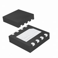
MAX3658AETA+T Maxim Integrated Products, MAX3658AETA+T Datasheet - Page 2

MAX3658AETA+T
Manufacturer Part Number
MAX3658AETA+T
Description
IC AMP TRANSIMPEDANCE 8-TDFN
Manufacturer
Maxim Integrated Products
Type
Transimpedance Amplifierr
Datasheet
1.MAX3658AETAT.pdf
(15 pages)
Specifications of MAX3658AETA+T
Applications
Optical Networks
Mounting Type
Surface Mount
Package / Case
8-TDFN Exposed Pad
Lead Free Status / RoHS Status
Lead free / RoHS Compliant
ABSOLUTE MAXIMUM RATINGS
Supply Voltage (V
Current into IN ....................................................................+5mA
Voltage at OUT+, OUT- ...................(V
Voltage FILT, MON .....................................-0.5V to (V
Continuous Power Dissipation (T
DC ELECTRICAL CHARACTERISTICS
(V
+25°C, unless otherwise noted.)
622Mbps, Low-Noise, High-Gain
Transimpedance Preamplifier
Stresses beyond those listed under “Absolute Maximum Ratings” may cause permanent damage to the device. These are stress ratings only, and functional
operation of the device at these or any other conditions beyond those indicated in the operational sections of the specifications is not implied. Exposure to
absolute maximum rating conditions for extended periods may affect device reliability.
Note 1: Accuracy is defined as 10
2
Supply Current
Input Bias Voltage
Transimpedance Linear Range
Small-Signal Transimpedance
Output Common-Mode Voltage
Differential Output Offset
Output Impedance
Maximum Output Voltage
Filter Resistor
Offset-Correction Disable
Threshold
Input Resistance
Nominal MON Current Gain
MON Output Voltage Range
MON Accuracy (Note 1)
CC
8-Lead TDFN (derate 24.4mW/°C above +85°C) ......1951.2mW
_______________________________________________________________________________________
= +2.97V to +3.63V, 150Ω load between OUT+ and OUT-, T
PARAMETER
CC
) ............................................-0.5V to +4.2V
A
= +85°C)
log
V
CC
(I
SYMBOL
OUT(MAX)
MON
ΔV
G
V
Z
R
Z
- 1.2V) to (V
I
V
MON
OUT
MON
CC
FILT
OUT
IN
21
/ I
IN
).
I
0.95 < linearity < 1.05
I
AC-coupled output
I
Single ended
I
I
I
Voltage applied at FILT
FILT = 0V
I
1µA ≤ I
2µA ≤ I
5µA ≤ I
IN
IN
IN
IN
IN
IN
MON
CC
CC
= 1µA
< 2µA
= 1.3mA
= 2mA
= 4µA
= 1.3mA
/ I
+ 0.5V)
+ 0.5V)
IN
IN
IN
IN
P-P
< 2µA
< 5µA
< 1mA
P-P
(I
IN
= 1mA, 3.3V, +25°C)
CONDITIONS
j
= -40°C to +100°C. Typical values are at V
Operating Temperature Range ...........................-40°C to +85°C
Operating Junction Temperature Range (die) ....-40°C to +150°C
Storage Temperature Range .............................-55°C to +150°C
Die Attach Temperature...................................................+400°C
Lead Temperature (soldering, 10s) .................................+300°C
MIN
15.7
-2.5
-1.5
150
300
0.8
60
15
-2
4
0
V
0.125
TYP
0.83
18.3
240
500
400
0.4
CC
20
±2
75
20
1
-
CC
= +3.3V and T
MAX
+2.5
+1.5
20.9
400
700
1.0
1.2
2.2
26
25
+2
90
UNITS
mV
µA
A/A
mA
mV
kΩ
kΩ
dB
Ω
Ω
Ω
V
V
V
V
P-P
P-P
A
=


