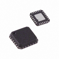
ADL5310ACP Analog Devices Inc, ADL5310ACP Datasheet - Page 5

ADL5310ACP
Manufacturer Part Number
ADL5310ACP
Description
IC LOGARITHMIC CONV DUAL 24LFCSP
Manufacturer
Analog Devices Inc
Type
Logarithmic Converterr
Datasheet
1.ADL5310ACPZ-REEL7.pdf
(20 pages)
Specifications of ADL5310ACP
Rohs Status
RoHS non-compliant
Design Resources
Interfacing ADL5315 to Translinear Logarithmic Amplifier (CN0056) Interfacing ADL5317 High Side Current Mirror to a Translinear Logarithmic Amplifier in an Avalanche Photodiode Power Detector
Applications
Fiber Optics
Mounting Type
Surface Mount
Package / Case
24-LFCSP
Available stocks
Company
Part Number
Manufacturer
Quantity
Price
Company:
Part Number:
ADL5310ACP-REEL7
Manufacturer:
TEXAS
Quantity:
550
Company:
Part Number:
ADL5310ACPZ
Manufacturer:
Analog Devices Inc
Quantity:
1 914
Part Number:
ADL5310ACPZ
Manufacturer:
ADI/亚德诺
Quantity:
20 000
Company:
Part Number:
ADL5310ACPZ-REEL7
Manufacturer:
CIRRUS
Quantity:
390
PIN CONFIGURATION AND FUNCTION DESCRIPTIONS
Table 3. Pin Function Descriptions
Pin No.
1, 6
2
3
4
5
7, 24
8, 9
10, 11, 20
12
13
14
15
16
17
18
19
21, 22
23
Mnemonic
VSUM
INP1
IRF1
IRF2
INP2
VREF
VPOS
VNEG
OUT2
SCL2
BIN2
LOG2
LOG1
BIN1
SCL1
OUT1
COMM
VRDZ
Function
Guard Pin. Used to shield the INP1 and INP2 input current lines, and for optional adjustment of the input
summing node potentials. Pin 1 and Pin 6 are internally shorted.
Channel 1 Numerator Input. Accepts (sinks) photodiode current I
such that photocurrent flows into INP1.
Channel 1 Denominator Input. Accepts (sinks) reference current, I
Channel 2 Denominator Input. Accepts (sinks) reference current, I
Channel 2 Numerator Input. Accepts (sinks) photodiode current I
such that photocurrent flows into INP2.
Reference Output Voltage of 2.5 V. Pin 7 and Pin 24 are internally shorted.
Positive Supply, (V
Optional Negative Supply, V
Applications sections. All VNEG pins must be connected externally.
Buffer Output for Channel 2.
Buffer Amplifier Inverting Input for Channel 2.
Buffer Amplifier Noninverting Input for Channel 2.
Output of the Logarithmic Front End for Channel 2.
Output of the Logarithmic Front End for Channel 1.
Buffer Amplifier Noninverting Input for Channel 1.
Buffer Amplifier Inverting Input for Channel 1.
Buffer Output for Channel 1.
Analog Ground. Pin 21 and Pin 22 are internally shorted.
Intercept Shift Reference Input. The top of a resistive divider network that offsets VLOG to position the
intercept. Normally connected to VREF; may also be connected to ground when bipolar outputs are to be
provided.
P
VSUM
VSUM
– V
INP1
INP2
IRF1
IRF2
N
) ≤ 12 V. Both pins must be connected externally.
Figure 2. 24-Lead LFCSP Pin Configuration
1
2
3
4
5
6
N
. These pins are usually grounded. For more details, see the General Structure and
24
7
PIN 1
INDICATOR
Rev. A | Page 5 of 20
23
DUAL LOG AMP
8
(Not to Scale)
ADL5310
TOP VIEW
22
9
21
10
20
11
19
12
18
17
16
15
14
13
SCL1
BIN1
LOG1
LOG2
BIN2
SCL2
PD1
PD2
RF1
RF2
. Usually connected to photodiode anode
. Usually connected to photodiode anode
.
.
ADL5310


