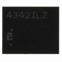
EL4342ILZA Intersil, EL4342ILZA Datasheet - Page 9

EL4342ILZA
Manufacturer Part Number
EL4342ILZA
Description
IC AMP MULTI TRPL 500MHZ 32QFN
Manufacturer
Intersil
Type
Analog Multiplexer/Ampr
Datasheet
1.EL4340IUZ.pdf
(13 pages)
Specifications of EL4342ILZA
Applications
4:1 Multiplexer-Amplifier
Number Of Circuits
3
-3db Bandwidth
500MHz
Slew Rate
870 V/µs
Current - Supply
46mA
Current - Output / Channel
135mA
Mounting Type
Surface Mount
Package / Case
32-VQFN Exposed Pad, 32-HVQFN, 32-SQFN, 32-DHVQFN
Package
32QFN EP
Maximum Propagation Delay Bus To Bus
0.9(Typ)@±5V ns
Maximum High Level Output Current
50 mA
Multiplexer Architecture
4:1
Power Supply Type
Dual
Lead Free Status / RoHS Status
Lead free / RoHS Compliant
Available stocks
Company
Part Number
Manufacturer
Quantity
Price
Company:
Part Number:
EL4342ILZA
Manufacturer:
Intersil
Quantity:
135
Company:
Part Number:
EL4342ILZA-T7
Manufacturer:
Intersil
Quantity:
1 800
AC Test Circuits
Figure 20A illustrates the optimum output load for testing AC
performance. Figure 20B illustrates the optimun output load
when connecting to 50Ω input terminated equipment.
Application Information
General
The EL4340, EL4342 triple 2:1 and 4:1 MUX amps are ideal
as the matrix element of high performance switchers and
routers. Key features include buffered high impedance
analog inputs and excellent AC performance at output loads
down to 150Ω for video cable-driving. The unity-gain current
feedback output amplifiers are stable operating into
capacitive loads and bandwidth is optimized with a load of
5pF in parallel with a 500Ω. Total output capacitance can be
FIGURE 20B. TEST CIRCUIT FOR MEASURING WITH 50Ω OR
FIGURE 20C. BACKLOADED TEST CIRCUIT FOR VIDEO CABLE
FIGURE 20A. TEST CIRCUIT WITH OPTIMAL OUTPUT LOAD
V
V
IN
IN
50Ω
75Ω
50Ω
75Ω
V+ SUPPLY
V- SUPPLY
OR
OR
EL4340, EL4342
EL4340, EL4342
SIGNAL
POWER
LOGIC
DE-COUPLING
GND
CAPS
75Ω INPUT TERMINATED EQUIPMENT
APPLICATION. BANDWIDTH AND LINEARITY
FOR R
V
IN
50Ω
75Ω
OR
FIGURE 20. TEST CIRCUITS
EL4340, EL4342
C
5
C
5pF
L
P
L
L
LESS THAN 500Ω WILL BE DEGRADED.
F
475Ω
50Ω OR 75Ω
R
R
S
S
9
C
5
L
50Ω
75Ω
P
OR
F
PROTECTION
SCHOTTKY
FIGURE 21. SCHOTTKY PROTECTION CIRCUIT
500Ω
R
L
EQUIPMENT
EQUIPMENT
50Ω
75Ω
50Ω
75Ω
OR
OR
TEST
TEST
GND
S0
IN0
IN1
EL4340, EL4342
V+
V-
V+
V-
V+
V-
split between the PCB capacitance and an external load
capacitor.
Ground Connections
For the best isolation and crosstalk rejection, all GND pins
and NIC pins must connect to the GND plane.
Control Signals
S0, S1, ENABLE, LE, HIZ - These are binary coded,
TTL/CMOS compatible control inputs. The S0, S1 pins select
the inputs. All three amplifiers are switched simultaneously
from their respective inputs. The ENABLE, LE, HIZ pins are
used to disable the part to save power, latch in the last logic
state and three-state the output amplifiers, respectively. For
control signal rise and fall times less than 10ns the use of
termination resistors close to the part will minimize transients
coupled to the output.
Power-up Considerations
The ESD protection circuits use internal diodes from all pins
the V+ and V- supplies. In addition, a dV/dT- triggered clamp
is connected between the V+ and V- pins, as shown in the
Equivalent Circuits 1 through 4 section of the Pin Description
table. The dV/dT triggered clamp imposes a maximum
supply turn-on slew rate of 1V/µs. Damaging currents can
flow for power supply rates-of-rise in excess of 1V/µs, such
as during hot plugging. Under these conditions, additional
methods should be employed to ensure the rate of rise is not
exceeded.
Consideration must be given to the order in which power is
applied to the V+ and V- pins, as well as analog and logic
input pins. Schottky diodes (Motorola MBR0550T or
equivalent) connected from V+ to ground and V- to ground
(Figure 21) will shunt damaging currents away from the
internal V+ and V- ESD diodes in the event that the V+
supply is applied to the device before the V- supply.
If positive voltages are applied to the logic or analog video
input pins before V+ is applied, current will flow through the
internal ESD diodes to the V+ pin. The presence of large
decoupling capacitors and the loading effect of other circuits
connected to V+, can result in damaging currents through
the ESD diodes and other active circuits within the device.
Therefore, adequate current limiting on the digital and
analog inputs is needed to prevent damage during the time
the voltages on these inputs are more positive than V+.
V+
V-
CONTROL
LOGIC
V+
V-
OUT
EXTERNAL
CIRCUITS
October 18, 2010
FN7421.3


