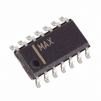
MAX4386EESD+ Maxim Integrated Products, MAX4386EESD+ Datasheet - Page 8

MAX4386EESD+
Manufacturer Part Number
MAX4386EESD+
Description
IC OP AMP R-R SNGL 14-SOIC
Manufacturer
Maxim Integrated Products
Datasheet
1.MAX4386EESD.pdf
(13 pages)
Specifications of MAX4386EESD+
Applications
Voltage Feedback
Output Type
Rail-to-Rail
Number Of Circuits
4
-3db Bandwidth
230MHz
Slew Rate
450 V/µs
Current - Supply
5.5mA
Current - Output / Channel
55mA
Voltage - Supply, Single/dual (±)
4.5 V ~ 5.5 V
Mounting Type
Surface Mount
Package / Case
14-SOIC (0.154", 3.90mm Width)
Number Of Channels
4
Voltage Gain Db
63 dB
Common Mode Rejection Ratio (min)
70 dB
Input Offset Voltage
20 mV
Operating Supply Voltage
5 V
Maximum Power Dissipation
667 mW
Maximum Operating Temperature
+ 85 C
Mounting Style
SMD/SMT
Minimum Operating Temperature
- 40 C
Lead Free Status / RoHS Status
Lead free / RoHS Compliant
The MAX4385E/MAX4386E are single/quad, 5V, rail-to-
rail, voltage-feedback amplifiers that employ current-
feedback techniques to achieve 450V/µs slew rates
and 230MHz bandwidths. High ±15kV ESD protection
guards against unexpected discharge. Excellent har-
monic distortion and differential gain/phase perfor-
mance make these amplifiers an ideal choice for a wide
variety of video and RF signal-processing applications.
The output voltage swings to within 50mV of each sup-
ply rail. Local feedback around the output stage
ensures low open-loop output impedance to reduce
gain sensitivity to load variations. The input stage per-
mits common-mode voltages beyond V
2.25V of the positive supply rail.
The MAX4385E/MAX4386E are internally compensated
for unity gain. When configured for unity gain, a 24Ω
resistor (R
AC performance. This resistor improves AC response
by reducing the Q of the parallel LC circuit formed by
the parasitic feedback capacitance and inductance.
The MAX4385E/MAX4386E are low-power, voltage-
feedback amplifiers featuring bandwidths up to
230MHz, 0.1dB gain flatness to 30MHz. They are
designed to minimize differential-gain error and differ-
ential-phase error to 0.02% and 0.01°, respectively.
They have a 14ns settling time to 0.1%, 450V/µs slew
rates, and output-current-drive capability of up to
50mA, making them ideal for driving video loads.
Select the gain-setting feedback (R
resistor values to fit your application. Large resistor val-
ues increase voltage noise and interact with the amplifi-
er’s input and PC board capacitance. This can
generate undesirable poles and zeros and decrease
bandwidth or cause oscillations. For example, a nonin-
verting gain-of-two configuration (R
resistors, combined with 8pF of amplifier input capaci-
tance and 1pF of PC board capacitance, causes a pole
at 35.4MHz. Since this pole is within the amplifier band-
width, it jeopardizes stability. Reducing the 1kΩ resis-
tors to 100Ω extends the pole frequency to 353.8MHz,
but could limit output swing by adding 200Ω in parallel
with the amplifier’s load resistor (Figures 1a
and 1b).
Low-Cost, 230MHz, Single/Quad Op Amps with
Rail-to-Rail Outputs and ±15kV ESD Protection
8
_______________________________________________________________________________________
F
Inverting and Noninverting Configurations
) in series with the feedback path optimizes
Applications Information
Detailed Description
Choosing Resistor Values
Unity-Gain Configuration
F
Video Line Driver
F
= R
) and input (R
EE
G
and to within
) using 1kΩ
G
)
These amplifiers operate from a single 5V power supply.
Bypass V
close to the pin as possible.
Maxim recommends using microstrip and stripline tech-
niques to obtain full bandwidth. To ensure that the PC
board does not degrade the amplifier’s performance,
design it for a frequency greater than 1GHz. Pay care-
ful attention to inputs and outputs to avoid large para-
sitic capacitance. Regardless of whether you use a
constant-impedance board, observe the following
design guidelines:
• Do not use wire-wrap boards; they are too inductive.
• Do not use IC sockets; they increase parasitic
• Use surface mount instead of through-hole compo-
• Use a PC board with at least two layers; it should be
• Keep signal lines as short and as straight as possi-
Figure 1b. Inverting Gain Configuration
Figure 1a. Noninverting Gain Configuration
capacitance and inductance.
nents for better high-frequency performance.
as free from voids as possible.
ble. Do not make 90° turns; round all corners.
Layout and Power-Supply Bypassing
CC
IN
to ground with 0.1µF and 2.2µF capacitors as
R
G
IN
R
G
MAX438_E
MAX438_E
R
F
V
OUT
V
R
OUT
F
= [1+ (R
= -(R
F
F
V
/ R
OUT
/ R
G
G
) V
V
)] V
OUT
IN
IN


