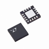
LT6559CUD#TRPBF Linear Technology, LT6559CUD#TRPBF Datasheet - Page 3

LT6559CUD#TRPBF
Manufacturer Part Number
LT6559CUD#TRPBF
Description
IC AMP VIDEO TRPL 16-QFN
Manufacturer
Linear Technology
Datasheet
1.LT6559CUDPBF.pdf
(16 pages)
Specifications of LT6559CUD#TRPBF
Applications
General Purpose
Number Of Circuits
3
-3db Bandwidth
300MHz
Slew Rate
800 V/µs
Current - Supply
4.6mA
Current - Output / Channel
100mA
Voltage - Supply, Single/dual (±)
4 V ~ 12 V, ±2 V ~ 6 V
Mounting Type
Surface Mount
Package / Case
16-WFQFN Exposed Pad
Lead Free Status / RoHS Status
Lead free / RoHS Compliant
Available stocks
Company
Part Number
Manufacturer
Quantity
Price
5V ELECTRICAL CHARACTERISTICS
temperature range, otherwise specifi cations are at T
otherwise noted. (Note 4)
SYMBOL
V
CMRR
PSRR
R
I
I
I
SR
t
t
t
t
os
t
dG
dP
±5V ELECTRICAL CHARACTERISTICS
SYMBOL
V
ΔV
I
I
e
+i
–i
R
C
C
V
V
V
operating temperature range, otherwise specifi cations are at T
unless otherwise noted. (Note 4)
OUT
S
⎯ E ⎯ N
ON
OFF
r
PD
S
IN
IN
n
, t
OUTL
OS
IN
OUT
INH
INL
OUTH
OL
IN
n
n
+
–
OS
f
/ΔT
PARAMETER
Maximum Output Voltage Swing, Low
Common Mode Rejection Ratio
Power Supply Rejection Ratio
Transimpedance, ΔV
Maximum Output Current
Supply Current per Amplifi er
Disable Supply Current per Amplifi er
Enable Pin Current
Slew Rate (Note 6)
Turn-On Delay Time (Note 7)
Turn-Off Delay Time (Note 7)
Small-Signal Rise and Fall Time
Propagation Delay
Small-Signal Overshoot
Settling Time
Differential Gain (Note 8)
Differential Phase (Note 8)
PARAMETER
Input Offset Voltage
Input Offset Voltage Drift
Noninverting Input Current
Inverting Input Current
Input Noise Voltage Density
Noninverting Input Noise Current
Density
Inverting Input Noise Current Density
Input Resistance
Input Capacitance
Output Capacitance
Input Voltage Range, High
Input Voltage Range, Low
Maximum Output Voltage Swing, High
OUT
/ΔI
IN
–
A
= 25°C. For each amplifi er: V
CONDITIONS
R
R
V
V
V
R
⎯ E ⎯ N Pin Voltage = 4.5V, R
A
R
R
R
V
R
V
R
V
0.1%, A
150Ω, V
R
R
CONDITIONS
f = 1kHz, R
f = 1kHz
f = 1kHz
V
Amplifi er Enabled
Amplifi er Disabled
Amplifi er Disabled
V
R
L
L
CM
S
OUT
L
V
F
F
F
S
F
S
F
S
F
F
IN
S
L
= 150Ω
= 150Ω
= ±2V to ±5V, ⎯ E ⎯ N = V
= 0Ω
= R
= R
= R
= ±5V
= R
= ±5V
= R
= ±5V
= R
= R
= ±5V
= 100k
= 10, R
= ±3.5V
= 1.5V to 3.5V
= 1.5V to 3.5V, R
G
G
G
G
G
G
G
V
A
= 301Ω, R
= 301Ω, R
= 301Ω, R
= 301Ω, R
= 301Ω, R
S
= 301Ω, R
= 301Ω, R
= –1V, R
= 25°C. For each amplifi er: V
= ±5V
L
The
F
= 150Ω, V
= 1k, R
The
●
denotes specifi cations which apply over the specifi ed operating
F
●
L
L
L
L
L
L
L
= R
G
denotes specifi cations which apply over the specifi ed
= 150Ω, V
= 150Ω, V
= 150Ω, V
= 150Ω, V
= 150Ω, V
= 150Ω, V
= 150Ω, V
= 10Ω, R
L
S
G
= 150Ω
–
= ±5V
L
= 301Ω, R
= 150Ω
S
S
S
OUT
OUT
OUT
S
S
CM
= 0Ω
= ±5V
= ±5V
= ±5V
= ±5V
= 2.5V, V
= 1V
= 1V
= 1V
L
=
P-P
P-P
P-P
,
,
,
CM
S
●
●
●
●
= 0V, V
= 5V, ⎯ E ⎯ N = 0V, pulse tested, unless
MIN
MIN
3.5
4.0
40
56
40
S
= ±5V, ⎯ E ⎯ N = 0V, pulse tested,
1.05
0.13
0.10
–4.0
TYP
TYP
500
3.9
0.1
1.3
2.5
1.5
4.5
2.0
2.5
8.5
4.0
4.2
50
70
80
65
30
30
40
10
25
15
10
10
25
6
1
LT6559
MAX
MAX
–3.5
1.15
1.35
100
100
6.1
75
10
25
60
nV/√ ⎯ H ⎯ z
pA/√ ⎯ H ⎯ z
pA/√ ⎯ H ⎯ z
UNITS
UNITS
µV/°C
3
V/µs
6559f
DEG
MΩ
mA
mA
mV
kΩ
µA
µA
µA
dB
dB
µA
ns
ns
ns
ns
ns
pF
pF
pF
%
%
V
V
V
V
V


