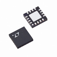
LT6559CUD#TRPBF Linear Technology, LT6559CUD#TRPBF Datasheet - Page 9

LT6559CUD#TRPBF
Manufacturer Part Number
LT6559CUD#TRPBF
Description
IC AMP VIDEO TRPL 16-QFN
Manufacturer
Linear Technology
Datasheet
1.LT6559CUDPBF.pdf
(16 pages)
Specifications of LT6559CUD#TRPBF
Applications
General Purpose
Number Of Circuits
3
-3db Bandwidth
300MHz
Slew Rate
800 V/µs
Current - Supply
4.6mA
Current - Output / Channel
100mA
Voltage - Supply, Single/dual (±)
4 V ~ 12 V, ±2 V ~ 6 V
Mounting Type
Surface Mount
Package / Case
16-WFQFN Exposed Pad
Lead Free Status / RoHS Status
Lead free / RoHS Compliant
Available stocks
Company
Part Number
Manufacturer
Quantity
Price
APPLICATIONS INFORMATION
internal capacitance. At a gain of 2 with 301Ω feedback
and gain resistors and ±5V supplies, the output slew rate
is typically 800V/µs. Larger feedback resistors will reduce
the slew rate as will lower supply voltages.
Enable/Disable
Each amplifi er of the LT6559 has a unique high imped-
ance, zero supply current mode which is controlled by its
own ⎯ E ⎯ N pin. These amplifi ers are designed to operate with
CMOS logic; the amplifi ers draw 0.1µA of current when
these pins are high or fl oated. To activate each amplifi er,
its ⎯ E ⎯ N pin is normally pulled to a logic low. However, sup-
ply current will vary as the voltage between the V
and ⎯ E ⎯ N is varied. As seen in Figure 1, +I
(V
than 3V. For normal operation, it is important to keep the
⎯ E ⎯ N pin at least 3V below the V
3V is used, for the amplifi er to remain enabled at all times
the ⎯ E ⎯ N pin should be tied to the V
current is approximately 30µA when activated. If using
CMOS open-drain logic, an external 1k pull-up resistor is
recommended to ensure that the LT6559 remains disabled
regardless of any CMOS drain-leakage currents.
+
– V
⎯ E ⎯ N
), particularly when the voltage difference is less
5.0
4.5
4.0
3.5
3.0
2.5
2.0
1.5
1.0
0.5
0
0
T
V
A
+
Figure 1. +I
= 25°C
= 5V
1
2
V
–
V
= – 5V
+
3
S
– V
vs (V
+
EN
4
supply. If a V
(V)
–
+
V
–
supply. The enable pin
– V
5
= 0V
⎯ E ⎯ N
)
6
S
6559 F01
does vary with
+
7
of less than
+
supply
The enable/disable times are very fast when driven from
standard 5V CMOS logic. Each amplifi er enables in about
30ns (50% point to 50% point) while operating on ±5V
supplies (Figure 2). Likewise, the disable time is approxi-
mately 40ns (50% point to 50% point) (Figure 3).
Differential Input Signal Swing
To avoid any breakdown condition on the input transis-
tors, the differential input swing must be limited to ±5V.
In normal operation, the differential voltage between the
input pins is small, so the ±5V limit is not an issue. In
the disabled mode however, the differential swing can be
the same as the input swing, and there is a risk of device
breakdown if the input voltage range has not been properly
considered.
V
V
V
V
S
IN
S
IN
= ±5V
= ±5V
= 1V
= 1V
Figure 3. Amplifi er Disable Time, A
Figure 2. Amplifi er Enable Time, A
R
R
R
R
F
G
F
G
= 301Ω
= 301Ω
= 301Ω
= 301Ω
R
R
L
L
= 100Ω
= 100Ω
6559 F03
6559 F02
V
V
LT6559
= 2
= 2
2V
0V
5V
0V
2V
0V
5V
0V
OUTPUT
OUTPUT
EN
EN
9
6559f


