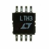
LT6206CMS8#TRPBF Linear Technology, LT6206CMS8#TRPBF Datasheet - Page 12

LT6206CMS8#TRPBF
Manufacturer Part Number
LT6206CMS8#TRPBF
Description
IC OP AMP VIDEO DUAL 3V 8-MSOP
Manufacturer
Linear Technology
Datasheet
1.LT6205CS5TRM.pdf
(18 pages)
Specifications of LT6206CMS8#TRPBF
Applications
Voltage Feedback
Output Type
Rail-to-Rail
Number Of Circuits
2
Slew Rate
600 V/µs
Current - Supply
4mA
Current - Output / Channel
60mA
Voltage - Supply, Single/dual (±)
2.7 V ~ 12.6 V, ±1.35 V ~ 6.3 V
Mounting Type
Surface Mount
Package / Case
8-TSSOP, 8-MSOP (0.118", 3.00mm Width)
Lead Free Status / RoHS Status
Lead free / RoHS Compliant
Available stocks
Company
Part Number
Manufacturer
Quantity
Price
APPLICATIONS INFORMATION
LT6205/LT6206/LT6207
Amplifi er Characteristics
Figure 1 shows a simplifi ed schematic of the LT6205/
LT6206/LT6207. The input stage consists of transistors
Q1 to Q8 and resistor R1. This topology allows for high
slew rates at low supply voltages. The input common
mode range extends from ground to typically 1.75V from
V
a current source. There are back-to-back series diodes,
D1 to D4, across the + and – inputs of each amplifi er to
limit the differential voltage to ±1.4V. R
through these diodes if the input differential voltage exceeds
±1.4V. The input stage drives the degeneration resistors of
PNP and NPN current mirrors, Q9 to Q12, which convert
the differential signals into a single-ended output. The
complementary drive generator supplies current to the
output transistors that swing from rail-to-rail.
The current generated through R1, divided by the capacitor
CM, determines the slew rate. Note that this current, and
hence the slew rate, are proportional to the magnitude
of the input step. The input step equals the output step
divided by the closed loop gain. The highest slew rates
are therefore obtained in the lowest gain confi gurations.
The Typical Performance Characteristics curve of Slew
Rate vs Closed-Loop Gain shows the details.
ESD
The LT6205/LT6206/LT6207 have reverse-biased ESD
protection diodes on all inputs and outputs as shown in
Figure 1. If these pins are forced beyond either supply
unlimited current will fl ow through these diodes. If the
current is transient, and limited to 25mA or less, no dam-
age to the device will occur.
Layout and Passive Components
With a gain bandwidth product of 100MHz and a slew rate
of 450V/μs the LT6205/LT6206/LT6207 require special
attention to board layout and supply bypassing. Use a
ground plane, short lead lengths and RF quality low ESR
supply bypass capacitors. The positive supply pin should
be bypassed with a small capacitor (typically 0.01μF to
0.1μF) within 0.25 inches of the pin. When driving heavy
loads, an additional 4.7μF electrolytic capacitor should be
used. When using split supplies, the same is true for the
12
CC
, and is limited by 2 VBEs plus a saturation voltage of
IN
limits the current
negative supply pin. For optimum performance all feedback
components and bypass capacitors should be contained
in a 0.5 inch by 0.5 inch area. This helps ensure minimal
stray capacitances.
The parallel combination of the feedback resistor and gain
setting resistor on the inverting input can combine with
the input capacitance to form a pole which can degrade
stability. In general, use feedback resistors of 1k or less.
Capacitive Load
The LT6205/LT6206/LT6207 are optimized for wide band-
width video applications. They can drive a capacitive load
of 20pF in a unity-gain confi guration. When driving a
larger capacitive load, a resistor of 10Ω to 50Ω should
be connected between the output and the capacitive load
to avoid ringing or oscillation. The feedback should still
be taken from the output pin so that the resistor will
isolate the capacitive load and ensure stability. The Typi-
cal Performance Characteristics curves show the output
overshoot when driving a capacitive load with different
series resistors.
Video Signal Characteristics
Composite video is the most commonly used signal in
broadcast grade products and includes luma (or lumi-
nance, the intensity information), chroma (the colorimetry
information) and sync (vertical and horizontal raster tim-
ing) elements combined into a single signal, NTSC and
PAL being the common formats. Component video for
entertainment systems include separate signal(s) for the
luma and chroma (i.e., Y/C or YPbPr) with sync generally
applied to the luma channel (Y signal). In some instances,
native RGB signals (separate intensity information for each
primary color: red, green, blue) will have sync included as
well. All the signal types that include sync are electrically
similar from a voltage-swing standpoint, though various
timing and bandwidth relationships exist depending on
the applicable standard.
The typical video waveforms that include sync (includ-
ing full composite) are specifi ed to have nominal 1V
amplitude. The lower 0.3V is reserved for sync tips that
carry timing information, and by being at a lower potential
than all the other information, represents blacker-than-
620567fc
P-P


