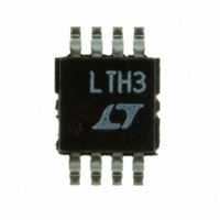
LT6206CMS8#TRPBF Linear Technology, LT6206CMS8#TRPBF Datasheet - Page 13

LT6206CMS8#TRPBF
Manufacturer Part Number
LT6206CMS8#TRPBF
Description
IC OP AMP VIDEO DUAL 3V 8-MSOP
Manufacturer
Linear Technology
Datasheet
1.LT6205CS5TRM.pdf
(18 pages)
Specifications of LT6206CMS8#TRPBF
Applications
Voltage Feedback
Output Type
Rail-to-Rail
Number Of Circuits
2
Slew Rate
600 V/µs
Current - Supply
4mA
Current - Output / Channel
60mA
Voltage - Supply, Single/dual (±)
2.7 V ~ 12.6 V, ±1.35 V ~ 6.3 V
Mounting Type
Surface Mount
Package / Case
8-TSSOP, 8-MSOP (0.118", 3.00mm Width)
Lead Free Status / RoHS Status
Lead free / RoHS Compliant
Available stocks
Company
Part Number
Manufacturer
Quantity
Price
APPLICATIONS INFORMATION
black intensity, thereby causing scan retrace activity to be
invisible on a CRT. The black level of the waveform is at
(or set up very slightly above) the upper limit of the sync
information. Waveform content above the black level is
intensity information, with peak brightness represented
at the maximum signal level. In the case of composite
video, the modulated color subcarrier is superimposed on
the waveform, but the dynamics remain inside the 1V
limit (a notable exception is the chroma ramp used for
differential-gain and differential-phase measurements,
which can reach 1.15V
DC-Coupled Video Amplifi er Considerations
Typically video amplifi ers drive cables that are series
terminated (back-terminated) at the source and load-ter-
minated at the destination with resistances equal to the
cable characteristic impedance, Z
confi guration forms a 2:1 resistor divider in the cabling
that must be accounted for in the driver amplifi er by
delivering 2V
150Ω). Driving the cable can require more than 13mA
while the output is approaching the saturation limits of the
amplifi er output. The absolute minimum supply is: V
2 + V
3.3V as shown on the front page of this data sheet, with
exceptionally low V
design margin of 0.45V. The design margin must be large
enough to include supply variations and DC bias accuracy
for the DC-coupled video input.
Handling AC-Coupled Video Signals
AC-coupled video inputs are intrinsically more diffi cult to
handle than those with DC-coupling because the average
signal voltage of the video waveform is effected by the
picture content, meaning that the black level at the amplifi er
wanders with scene brightness. The wander is measured
as 0.56V for a 1V
fi eld to white fi eld and vice-versa, so an additional 1.12V
allowance must be made in the amplifi er supply (assum-
ing gain of 2, so V
an LT6205 operating on 5V has a conservative design
margin of 1.03V. The amplifi er output (for gain of 2) must
swing +1.47V to –1.65V around the DC-operating point,
so the biasing circuitry needs to be designed accordingly
for optimal fi delity.
OH
+V
OL
. For example, the LT6206 dual operating on
P-P
P-P
output into an effective 2 • Z
MIN
OH
NTSC waveform changing from black
≤ 0.5V and V
= 3.12 + V
P-P
).
OH
0
OL
(usually 75Ω). This
+V
≤ 0.35V, provides a
OL
). For example,
0
load (e.g.,
MIN
P-P
=
Clamped AC-Input Cable Driver
A popular method of further minimizing supply require-
ments with AC-coupling is to employ a simple clamping
scheme, as shown in Figure 2. In this circuit, the LT6205
operates from 3.3V by having the sync tips control the
charge on the coupling capacitor C1, thereby reducing
the black level input wander to ≈ 0.07V. The only minor
drawback to this circuit is the slight sync tip compression
(≈ 0.025V at input) due to the diode conduction current,
though the picture content remains full fi delity. This circuit
has nearly the design margin of its DC-coupled counter-
part, at 0.31V (for this circuit, V
The clamp diode anode bias is selected to set the sync tip
output voltage at or slightly above V
YPbPr to RGB Component Video Converter
The back page application uses the LT6207 quad to imple-
ment a minimum amplifi er count topology to transcode
consumer component video into RGB. In this circuit, signals
only pass through one active stage from any input to any
output, with passive additions being performed by the
cable back-termination resistors. The compromise in using
passive output addition is that the amplifi er outputs must
be twice as large as that of a conventional cable driver. The
Y-channel section also has the demanding requirement that
it single-handedly drives all three outputs to full brightness
during times of white content, so a helper current source
is used to assure unclipped video when operating from
±5V supplies. This circuit maps sync-on-Y to sync on all
the RGB channels, and for best results should have input
black levels at 0V nominal to prevent clipping.
LT6205/LT6206/LT6207
MIN
OL
= 2.14 + V
.
OH
13
+V
620567fc
OL
).


