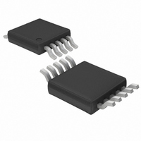
LT6551CMS Linear Technology, LT6551CMS Datasheet - Page 5

LT6551CMS
Manufacturer Part Number
LT6551CMS
Description
IC AMP VIDEO QUAD 3.3V 10-MSOP
Manufacturer
Linear Technology
Datasheet
1.LT6550CMS.pdf
(16 pages)
Specifications of LT6551CMS
Applications
Voltage Feedback
Output Type
Rail-to-Rail
Number Of Circuits
4
-3db Bandwidth
90MHz
Slew Rate
600 V/µs
Current - Supply
8.5mA
Current - Output / Channel
60mA
Voltage - Supply, Single/dual (±)
3 V ~ 12.6 V
Mounting Type
Surface Mount
Package / Case
10-TFSOP, 10-MSOP (0.118", 3.00mm Width)
Lead Free Status / RoHS Status
Contains lead / RoHS non-compliant
Available stocks
Company
Part Number
Manufacturer
Quantity
Price
Company:
Part Number:
LT6551CMS
Manufacturer:
LT
Quantity:
10 000
Part Number:
LT6551CMS
Manufacturer:
LINEAR/凌特
Quantity:
20 000
Part Number:
LT6551CMS#PBF
Manufacturer:
LINEAR/凌特
Quantity:
20 000
Company:
Part Number:
LT6551CMS#TRPBF
Manufacturer:
LT
Quantity:
903
Part Number:
LT6551CMS#TRPBF
Manufacturer:
LINEAR/凌特
Quantity:
20 000
±5V ELECTRICAL CHARACTERISTICS
Note 1: Absolute Maximum Ratings are those values beyond which the life
of a device may be impaired.
Note 2: A heat sink may be required to keep the junction temperature
below absolute maximum. This depends on the power supply voltage and
how many amplifiers are shorted.
Note 3: The LT6550C/LT6551C are guaranteed to meet specified
performance from 0°C to 70°C and are designed, characterized and
expected to meet specified performance from –40°C to 85°C but are not
tested or QA sampled at these temperatures. The LT6550I/LT6551I are
guaranteed to meet specified performance from – 40°C to 85°C.
the specified temperature range, otherwise specifications are at T
otherwise noted.
PARAMETER
Supply Current per Amplifier
Slew Rate
Small Signal –3dB Bandwidth
Gain Flatness
Gain Matching
Settling Time to 3%
Settling Time to 1%
% Overshoot
Differential Gain
Differential Phase
Channel Separation
5V/3.3V TYPICAL PERFOR A CE CHARACTERISTICS
V
EE
14
12
10
8
6
4
2
0
(Pin 5) = 0V (LT6550), GND (Pin 5) = 0V (LT6551)
0
Supply Current Per Amplifier vs
Supply Voltage
V
R
GND = 0V
IN
L
1
= ∞
= 0.75V
2
3
4
T
A
V
CC
= 25°C
5
(V)
6
7
T
T
A
A
= 125°C
8
= –55°C
6550/51 G01
9
10
W
CONDITIONS
R
Measured from –2V to 2V
R
Less than 0.25dB
Any One Channel to Any Other Channel
R
R
V
R
R
Measured at 10MHz
3.5
3.0
2.5
2.0
1.5
1.0
0.5
OUT
L
L
L
L
L
L
0
= 150Ω, V
= 150Ω
= 150Ω, V
= 150Ω, V
= 150Ω, Black Level = 0V at Device Output
= 150Ω, Black Level = 0V at Device Output
0
Output Voltage vs Input Voltage
V
R
U
= 1V to 2.5V, R
S
L
0.2
= 3.3V, 0V
= 150Ω
0.4
OUT
OUT
OUT
0.6 0.8
= –3V to 3V,
= 1V to 2.5V
= 1V to 2.5V
A
(LT6550 Only) The
L
V
= 25°C. V
IN
= 150Ω
1.0
Note 4: Thermal resistance varies depending upon the amount of PC board
metal attached to Pin 5 of the device. θ
board covered with 2oz copper on both sides.
Note 5: Gain is measured by changing the input voltage, and dividing the
change in output voltage by the change in input voltage.
Note 6: Minimum supply voltage is guaranteed by the PSRR test.
Note 7: The supply current specification includes additional output current
through the internal feedback and gain resistor.
Note 8: Guaranteed by correlation to slew rate at 5V and ±5V.
Note 9: The inputs are protected from ESD with diodes to the supplies.
Note 10: Noise is input referred, including internal gain resistors.
(V)
T
A
1.2
= 125°C
1.4
S
T
= ±5V, V
A
1.6
T
A
= –55°C
= 25°C
6550/51 G02
1.8
●
2.0
IN
denotes the specifications which apply over
= 0V (Pins 1,2,3) V
–10
–11
–12
–13
–14
–15
–16
–17
–18
–19
–20
●
●
–50
Input Bias Current vs
Temperature
V
V
S
OUT
LT6550/LT6551
MIN
400
300
= 5V, 0V
–25
JA
= 2.5V
is specified for a 2500mm
GND
0
TEMPERATURE (°C)
0.15
0.15
0.09
TYP
600
8.5
20
30
90
30
60
5
= 0V (Pin 4) unless
25
50
MAX
10.5
12
75
100
2
6550/51 G03
UNITS
65501fa
test
5
V/µs
V/µs
MHz
MHz
Deg
mA
mA
125
dB
dB
ns
ns
%
%


