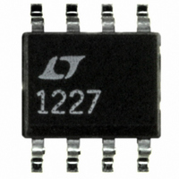
LT1227CS8#TR Linear Technology, LT1227CS8#TR Datasheet - Page 8

LT1227CS8#TR
Manufacturer Part Number
LT1227CS8#TR
Description
IC AMP VID DIFF CURR FDBK 8SOIC
Manufacturer
Linear Technology
Datasheet
1.LT1227CN8PBF.pdf
(12 pages)
Specifications of LT1227CS8#TR
Applications
Current Feedback
Number Of Circuits
1
-3db Bandwidth
140MHz
Slew Rate
1100 V/µs
Current - Supply
10mA
Current - Output / Channel
60mA
Voltage - Supply, Single/dual (±)
4 V ~ 30 V, ±2 V ~ 15 V
Mounting Type
Surface Mount
Package / Case
8-SOIC (0.154", 3.90mm Width)
Lead Free Status / RoHS Status
Contains lead / RoHS non-compliant
Available stocks
Company
Part Number
Manufacturer
Quantity
Price
LT1227
Capacitance on the Inverting Input
Current feedback amplifiers require resistive feedback
from the output to the inverting input for stable operation.
Take care to minimize the stray capacitance between the
output and the inverting input. Capacitance on the invert-
ing input to ground will cause peaking in the frequency
response (and overshoot in the transient response), but it
does not degrade the stability of the amplifier.
Capacitive Loads
The LT1227 can drive capacitive loads directly when the
proper value of feedback resistor is used. The graph of
Maximum Capacitive Load vs Feedback Resistor should
be used to select the appropriate value. The value shown
is for 5dB peaking when driving a 1k load at a gain of 2. This
is a worst case condition, the amplifier is more stable at
higher gains and driving heavier loads. Alternatively, a
small resistor (10 to 20 ) can be put in series with the
output to isolate the capacitive load from the amplifier
output. This has the advantage that the amplifier band-
width is only reduced when the capacitive load is present
and the disadvantage that the gain is a function of the load
resistance.
Power Supplies
The LT1227 will operate from single or split supplies from
use equal value split supplies, however the offset voltage
A
8
2V (4V total) to 15V (30V total). It is not necessary to
PPLICATI
V
OUT
Small-Signal Rise Time, A
O
U
R
S
F
= 1k, R
I FOR ATIO
U
G
= 1k, R
L
= 100
W
V
= +2
U
AI01
and inverting input bias current will change. The offset
voltage changes about 500 V per volt of supply mis-
match. The inverting bias current can change as much as
5.0 A per volt of supply mismatch, though typically the
change is less than 0.5 A per volt.
Slew Rate
The slew rate of a current feedback amplifier is not
independent of the amplifier gain configuration the way
slew rate is in a traditional op amp. This is because both the
input stage and the output stage have slew rate limitations.
In the inverting mode, and for higher gains in the
noninverting mode, the signal amplitude between the
input pins is small and the overall slew rate is that of the
output stage. For gains less than ten in the noninverting
mode, the overall slew rate is limited by the input stage.
The input stage slew rate of the LT1227 is approximately
125V/ s and is set by internal currents and capacitances.
The output slew rate is set by the value of the feedback
resistors and the internal capacitances. At a gain of ten
with a 1k feedback resistor and 15V supplies, the output
slew rate is typically 1100V/ s. Larger feedback resistors
will reduce the slew rate as will lower supply voltages,
similar to the way the bandwidth is reduced.
The graph of Maximum Undistorted Output vs Frequency
relates the slew rate limitations to sinusoidal inputs for
various gain configurations.
V
OUT
Large-Signal Transient Response, A
R
F
= 910 , R
G
= 100 , R
L
= 400
V
= +10
AI02


