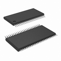
LM8207MTX/NOPB National Semiconductor, LM8207MTX/NOPB Datasheet - Page 16

LM8207MTX/NOPB
Manufacturer Part Number
LM8207MTX/NOPB
Description
IC BUFFER/DVR/VREF 48-TSSOP
Manufacturer
National Semiconductor
Datasheet
1.LM8207MTNOPB.pdf
(22 pages)
Specifications of LM8207MTX/NOPB
Applications
TFT-LCD Panels: Gamma Buffer, VCOM Driver
Output Type
Rail-to-Rail
Number Of Circuits
18
-3db Bandwidth
2MHz
Slew Rate
1 V/µs
Current - Supply
6.5mA
Current - Output / Channel
50mA
Voltage - Supply, Single/dual (±)
6 V ~ 16 V
Mounting Type
Surface Mount
Package / Case
48-TFSOP (0.240", 6.10mm Width)
Lead Free Status / RoHS Status
Lead free / RoHS Compliant
Other names
LM8207MTX
www.national.com
Application Section
Changing the gamma correction curve, in combination with
the load of the column drivers can impact the behavior of the
gamma buffers. Gamma buffers 1 and 2 are designed for
operating voltages near V
the column drivers. Gamma buffers 17 and 18 are designed
for operating voltages near V
Buffers 3 to 16 are designed to operate in the mid-voltage
range and can sink or source current. Under special circum-
stances, by increasing the voltage gap between gamma
buffer 1 and gamma buffer 2, in combination with a low
impedance load of the column driver between these outputs,
the output of buffer 2 has to sink more current than possible,
and can saturate. This will result in a setting error of the
inputs of the column driver.
For buffer 17 and 18 an identical situation can occur, by
increasing the operating voltage range of buffer 17 with
respect to buffer 18.
A simple and cost effective solution is to lower the resistance
between buffer 2 and 3 or buffer 16 and 17, using an
additional by-pass resistor R
Figure 10. This will not affect the desired voltage levels, and
buffer 3 which has a larger linear output current spec will sink
the current instead of buffer 2. The resistor value R
calculated by the voltage drop divided by the current. The
resistor value should be low enough to sink this current,
otherwise buffer 2 and/or buffer 17 will still saturate.
1
2
3
4
5
6
7
8
9
10
11
12
13
14
15
16
17
18
TABLE 1. Resistor Values for Defining the Gamma
VGMA
Node
11.59
11.38
9.18
8.51
7.84
7.41
7.13
6.15
6.07
5.90
5.82
4.84
4.56
4.13
3.46
2.73
0.54
0.33
VGMA Voltage
Gamma Curve Definition
Correction Curve
DD
, and will source the current into
S
. This method is presented in
SS
210
2200
670
670
430
280
980
80
170
80
980
280
430
670
730
2190
210
330
Calculated Resistance (Ω)
and will sink this current.
(Continued)
S
can be
16
GAMMA VOLTAGE ACCURACY
Adding buffers to the tabs of the gamma correction resistor
chain will make the values more independent of the load
variations. Unfortunately, there are some other effects that
will influence the gamma values. The following effects deter-
mine the accuracy of each gamma voltage.
Major effects are:
• Variation of the internal voltage reference. This can be
• Variation of the feedback resistors used for setting the
• The accuracy of the resistors obtained from the gamma
• Output offset voltage (V
Minor effects are:
• Input current (I
found in the Electrical Characteristics Table. This is the
maximum variation between parts.
output voltage of the voltage reference (OUT_V
ing high accuracy resistors will result in a small variation
of the output voltage between different boards
correction voltage curve. The gamma correction curve
will be affected by the accuracy of the resistors. This will
vary over different boards. Temperature variations will not
affect this curve.
V
gamma correction curve. The contribution of V
higher for the buffers driving the lower gamma voltages.
the input current (I
temperature changes, will affect the gamma correction
voltages.
FIGURE 10. Using additional by-pass resistor to
OS
(output offset voltage) of the buffers, will affect the
increase current sinking capability
BIAS
BIAS
) of the gamma buffers. Variations of
) of the gamma buffers caused by
OS
) of the buffers. Variations of
REF
20137946
OS
). Us-
is


