LM8207MTX/NOPB National Semiconductor, LM8207MTX/NOPB Datasheet - Page 3
LM8207MTX/NOPB
Manufacturer Part Number
LM8207MTX/NOPB
Description
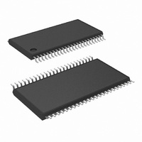
IC BUFFER/DVR/VREF 48-TSSOP
Manufacturer
National Semiconductor
Datasheet
1.LM8207MTNOPB.pdf
(22 pages)
Specifications of LM8207MTX/NOPB
Applications
TFT-LCD Panels: Gamma Buffer, VCOM Driver
Output Type
Rail-to-Rail
Number Of Circuits
18
-3db Bandwidth
2MHz
Slew Rate
1 V/µs
Current - Supply
6.5mA
Current - Output / Channel
50mA
Voltage - Supply, Single/dual (±)
6 V ~ 16 V
Mounting Type
Surface Mount
Package / Case
48-TFSOP (0.240", 6.10mm Width)
Lead Free Status / RoHS Status
Lead free / RoHS Compliant
Other names
LM8207MTX


I
PSRR
V
BW_V
SR_ V
T_
V
V
I
V
I
I
PSRR
Voltage Reference Section
V
Reg
V
V
I
TC_V
I
PSRR
Miscellaneous
I
OUT
BIAS
OUT
OUT
IN
OUT
S
16V Electrical Characteristics
COM
IN
OUT
OS
REF
REF_ACC
REF_MAX
Unless otherwise specified, all limits guaranteed for T
Buffers). Boldface limits apply at the temperature extremes. (Note 5)
Note 1: Absolute Maximum Ratings indicate limits beyond which damage to the device may occur. Operating Ratings indicate conditions for which the device is
intended to be functional, but specific performance is not guaranteed. For guaranteed specifications, see the Electrical Characteristics tables.
Note 2: When the output of the V
Note 3: Human body model, 1.5 kΩ in series with 100 pF. Machine model, 0Ω in series with 200 pF
Note 4: The maximum power dissipation is a function of T
is P
Note 5: Electrical Table values apply only for factory testing conditions at the temperature indicated. Factory testing condition result in very limited self-heating of
the device such that T
_V
REC
Symbol
_V
_V
LOAD
_Gamma
_
_SC_V
_V
_V
D
REF
_V
LIN
REF
COM
Driver
COM
_V
= (T
COM
COM
REF
COM
COM
_V
COM
J(MAX)
COM
COM
– T
Linear Output Current
(Note 10)
Power Supply Rejection Ratio
Bandwidth
Slew Rate (Note 8)
Output Recovery Time (Note 9)
Input Voltage Range
Output Voltage Range
Input Bias Current
Input Offset Voltage
Linear Output Current
(Notes 10, 11)
Short Circuit Output Current
(Notes 11, 12)
Power Supply Rejection Ratio
Voltage
Load Regulation
Voltage Accuracy
Max Programming Range
Input Bias Current
Temperature Stability
Max Output Current
Power Supply Rejection Ratio
(Line Regulation)
Supply Current
A
)/θ
J
= T
JA
. All numbers apply for packages soldered directly onto a PC board.
A
. No guarantee of parametric performance is indicated in the electrical table under conditions of internal self-heating where T
Parameter
COM
buffer exceeds the supply rails, while sinking or sourcing 100 mA, the V
Buffer 1-2
Buffer 3-8 & 11-16
Buffer 9
Buffer 10
Buffer 17-18
V
Positive
Negative
No Load
Within V
Voltage Range
V
Sourcing
Sinking
Sourcing
Sinking
V
No Load
I
No Load, V
I
Within V
Range
Sourcing, V
OUT
OUT
J(MAX)
DD
IN
DD
(Continued)
= 8 V
J
- V
- V
= 0 to 10 mA
= 4 mA
, θ
= 25˚C, V
SS
SS
JA
COM
REF
Conditions
= 6V to 16V
= 6V to 16V
and T
REF
OUT
Output Voltage
Buffer Output
3
= 1.295V
A
= 1.295 V
DD
. The maximum allowable power dissipation at any ambient temperature
= 16V, V
Sourcing
Sinking
Sourcing
Sinking
Sourcing
Sinking
Sourcing
Sinking
Sourcing
Sinking
Positive
Negative
SS
= 0V, & C
V
(Note 6)
DD
1.28
Min
220
220
0.2
3.5
4.5
3.5
0.2
4.5
20
10
15
23
20
75
75
70
–1.0
COM
LOAD
output is susceptible to latch.
V
V
V
V
= 100 pF (Gamma & V
(Note 7)
DD
DD
SS
SS
1.295
0.33
24.5
34.8
0.33
0.14
Typ
V
200
160
150
300
300
5.5
9.4
5.5
4.5
6.5
46
27
50
88
10
50
88
10
70
71
80
1
1
DD
+0.9
+0.6
–0.7
−0.3
V
(Note 6)
SS
Max
1.31
8.5
9.5
10
50
+1.2
www.national.com
COM
J
mV/mA
ppm/˚C
Units
>
MHz
V/µs
mA
mV
mA
mA
mA
mA
dB
nA
dB
nA
dB
ns
%
V
V
V
V
T
A
.
Related parts for LM8207MTX/NOPB
Image
Part Number
Description
Manufacturer
Datasheet
Request
R

Part Number:
Description:
IC,TV/VIDEO CIRCUIT,LCD Video Circuit,TSSOP,48PIN,PLASTIC
Manufacturer:
National Semiconductor
Datasheet:

Part Number:
Description:
IC BUFFER+VCOM+VREF 18CH 48TSSOP
Manufacturer:
National Semiconductor
Datasheet:
Part Number:
Description:
IC,TV/VIDEO CIRCUIT,LCD Video Circuit,TSSOP,48PIN,PLASTIC
Manufacturer:
National Semiconductor
Datasheet:
Part Number:
Description:
National Semiconductor [8-Bit D/A Converter]
Manufacturer:
National Semiconductor
Datasheet:
Part Number:
Description:
National Semiconductor [Media Coprocessor]
Manufacturer:
National Semiconductor
Datasheet:
Part Number:
Description:
Digitally Controlled Tone and Volume Circuit with Stereo Audio Power Amplifier, Microphone Preamp Stage and National 3D Sound
Manufacturer:
National Semiconductor
Datasheet:
Part Number:
Description:
Digitally Controlled Tone and Volume Circuit with Stereo Audio Power Amplifier, Microphone Preamp Stage and National 3D Sound
Manufacturer:
National Semiconductor
Datasheet:
Part Number:
Description:
AC97 Rev 2 Codec with Sample Rate Conversion and National 3D Sound
Manufacturer:
National Semiconductor
Part Number:
Description:
Manufacturer:
National Semiconductor
Datasheet:
Part Number:
Description:
Manufacturer:
National Semiconductor
Datasheet:
Part Number:
Description:
General Purpose, Low Voltage, Low Power, Rail-to-Rail Output Operational Amplifiers
Manufacturer:
National Semiconductor
Datasheet:
Part Number:
Description:
8-bit 20 MSPS flash A/D converter.
Manufacturer:
National Semiconductor
Datasheet:
Part Number:
Description:
Low Noise Quad Operational Amplifier
Manufacturer:
National Semiconductor
Datasheet:
Part Number:
Description:
Quad Differential Line Receivers
Manufacturer:
National Semiconductor
Datasheet: