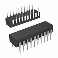
HA5024IPZ Intersil, HA5024IPZ Datasheet - Page 9

HA5024IPZ
Manufacturer Part Number
HA5024IPZ
Description
IC AMP VIDEO 125MHZ QUAD 20-PDIP
Manufacturer
Intersil
Specifications of HA5024IPZ
Applications
Current Feedback
Number Of Circuits
4
-3db Bandwidth
125MHz
Slew Rate
350 V/µs
Current - Supply
7.5mA
Current - Output / Channel
20mA
Voltage - Supply, Single/dual (±)
±4.5 V ~ 18 V
Mounting Type
Through Hole
Package / Case
20-DIP (0.300", 7.62mm)
Amplifier Type
High Slew Rate, High Speed, Video
Bandwidth
125 MHz
Common Mode Rejection Ratio
50
Current, Input Bias
4 μA
Current, Output
20 mA
Current, Supply
7.5 mA
Number Of Amplifiers
Quad
Package Type
PDIP-20
Temperature, Operating, Range
-40 to +85 °C
Time, Fall
6 ns
Time, Rise
6 ns
Voltage, Gain
65 dB
Voltage, Input
±5 V
Voltage, Noise
4.5 nV/sqrt Hz
Voltage, Offset
5 mV
Voltage, Output, High
+3 V
Voltage, Output, Low
-3 V
Voltage, Supply
36 V
Lead Free Status / RoHS Status
Lead free / RoHS Compliant
Available stocks
Company
Part Number
Manufacturer
Quantity
Price
Company:
Part Number:
HA5024IPZ
Manufacturer:
Intersil
Quantity:
234
Referring to Figure 10, both inputs are terminated in their
characteristic impedance; 75Ω is typical for video
applications. Since the drivers usually are terminated in their
characteristic impedance the input gain is 0.5, thus the
amplifiers, U
gain equal to one. Resistors R
gain, and if a different gain is desired R
according to the equation G = (1 + R
frequency response of the amplifier so you should refer to the
manufacturers data sheet before changing its value. R
and D
which configures U
both amplifiers from being active simultaneously. If this design
is extended to more channels the drive logic must be designed
1
are an asymmetrical charge/discharge time circuit
2
, are configured in a gain of +2 to set the circuit
CHANNEL
1
INPUT B
INPUT A
SWITCH
INHIBIT
as a break before make switch to prevent
2
9
and R
100K
R
U
R
6
75
1A
3
1B
/R
3
2
determine the amplifier
2
should be changed
). R
U
U
1C
1B
3
FIGURE 10. LOW IMPEDANCE MULTIPLEXER
sets the
R
75
1A
0.047µF
U
5
, C
D
1N4148
1D
2000
R
1A
C
5A
1
1A
HA5024
D
1N4148
2000
R
1B
5B
R
681
to be break before make. R
loop of the amplifier so that the large open loop amplifier
gain of U
output impedance while keeping the amplifier stable for all
values of load capacitance.
The circuit shown in Figure 10 was tested for the full range of
capacitor values with no oscillations being observed; thus,
problem one has been solved.The frequency and gain
characteristics of the circuit are now those of the amplifier
independent of any multiplexing action; thus, problem two
has been solved. The multiplexer transition time is
approximately 15µs with the component values shown.
(NOTE 17)
(NOTE 17)
100Ω
100Ω
R
2B
681
1A
C
0.047µF
1B
2
1
2
7
6
3
will present the load with a small closed loop
+
+
-
-
U
U
5
R
681
2A
2B
3A
R
681
16
10
13
4
3B
0.01µF
0.01µF
+5V
-5V
R
R
27
27
4B
4A
NOTES:
22. U
23. U
4
2
1
is enclosed in the feedback
: HA5022/24.
: CD4011.
OUTPUT
February 8, 2006
3550.6


