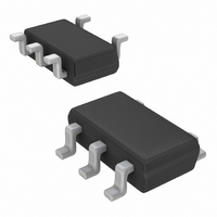
MAX1886EZK+T Maxim Integrated Products, MAX1886EZK+T Datasheet - Page 2

MAX1886EZK+T
Manufacturer Part Number
MAX1886EZK+T
Description
IC VCOM DRIVE BUFFER TSOT23-5
Manufacturer
Maxim Integrated Products
Datasheet
1.MAX1886EZKT.pdf
(7 pages)
Specifications of MAX1886EZK+T
Applications
TFT-LCD Panels: VCOM Driver
Number Of Circuits
1
Current - Supply
450µA
Current - Output / Channel
550mA
Voltage - Supply, Single/dual (±)
4.5 V ~ 13 V
Mounting Type
Surface Mount
Package / Case
SOT-23-5 Thin, TSOT-23-5
Lead Free Status / RoHS Status
Lead free / RoHS Compliant
ABSOLUTE MAXIMUM RATINGS
V
FB-, FB+, OUT to GND...............................-0.3V to (V
Continuous Power Dissipation (T
High-Current VCOM Drive Buffer
This device is constructed using a unique set of packaging techniques that impose a limit on the thermal profile the device can be exposed to during
board level solder attach and rework. Maxim recommends the use of the solder profiles recommended in the industry-standard specification, JEDEC
020A, paragraph 7.6, Table 3 for IR/VPR and convection reflow processes. Preheating, per this standard, is required. Hand or wave soldering is not
recommended.
Stresses beyond those listed under “Absolute Maximum Ratings” may cause permanent damage to the device. These are stress ratings only, and functional
operation of the device at these or any other conditions beyond those indicated in the operational sections of the specifications is not implied. Exposure to
absolute maximum rating conditions for extended periods may affect device reliability.
ELECTRICAL CHARACTERISTICS
(V
(Note 1)
Note 1: The MAX1886 is 100% production tested at T
Figure 1. Load Transient Test Circuit
2
REFERENCE
CC
V
V
Input Offset Voltage
Input Bias Current
Input Offset Current
Common-Mode Input Range
Power-Supply Rejection Ratio
Common-Mode Rejection Ratio
Gain-Bandwidth Product
Transconductance
Output Current Drive
Thermal Shutdown
Thermal Shutdown Hysteresis
VOLTAGE
CC
5-Pin Thin SOT23 (derate 7.1mW°C above +70°C) .....727mW
CC
CC
_______________________________________________________________________________________
to GND ............................................................-0.3V to +14V
= 10V, FB- = OUT, V
Input Supply Range
Supply Current
PARAMETER
5
4
FB+
MAX1886
= 5V, C
A
= +70°C)
SYMBOL
OUT
CMRR
1
3
2
PSRR
GBW
I
V
I
VOLTAGE
V
V
BIAS
SUPPLY
I
I
OUT
g
CC
OS
CC
CM
OS
m
= 0.47µF, T
0.47
0.47
R
L
V
+1.2V < V
|
+4.5V < V
+1.2V < V
Small signal
Small signal (±1mV overdrive)
Large signal (±30mV overdrive)
±100mV overdrive,
V
V
V
X
FB+
OUT
OS
CC
C
L
A
A
|
= +5V, no load
< 10mV over CMR
= 3V or 7V
+ 0.3V)
= -40°C to +85°C, unless otherwise noted. Typical values are at T
= +25°C. Specifications over temperature are guaranteed by design.
CM
CC
CM
< +13V, V
< +8.8V
< +8.8V
CONDITIONS
Operating Temperature Range ...........................-40°C to +85°C
Junction Temperature ......................................................+150°C
Storage Temperature Range .............................-65°C to +150°C
T
T
A
A
FB+
= -40°C to +85°C
= 0°C to +85°C
= +2.25V
±175
±250
-100
-100
MIN
4.5
1.2
70
70
-5
1/6πC
±550
TYP
450
170
0.3
10
15
L
V
MAX
1.2V
900
100
100
CC
13
5
-
A
= +25°C.)
UNITS
mV
mA
dB
µA
nA
nA
Hz
°C
°C
V
V
S


