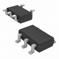
MAX1886EZK+T Maxim Integrated Products, MAX1886EZK+T Datasheet - Page 4

MAX1886EZK+T
Manufacturer Part Number
MAX1886EZK+T
Description
IC VCOM DRIVE BUFFER TSOT23-5
Manufacturer
Maxim Integrated Products
Datasheet
1.MAX1886EZKT.pdf
(7 pages)
Specifications of MAX1886EZK+T
Applications
TFT-LCD Panels: VCOM Driver
Number Of Circuits
1
Current - Supply
450µA
Current - Output / Channel
550mA
Voltage - Supply, Single/dual (±)
4.5 V ~ 13 V
Mounting Type
Surface Mount
Package / Case
SOT-23-5 Thin, TSOT-23-5
Lead Free Status / RoHS Status
Lead free / RoHS Compliant
The MAX1886 operational transconductance amplifier
(OTA) provides high-current output that is ideal for dri-
ving capacitive loads such as the backplane of a TFT
LCD panel. The positive feedback input, FB+, allows
common-mode biasing to mid-supply, or other VCOM
voltage.
The MAX1886 unity-gain bandwidth is GBW = g
where g
Transconductance is the ratio of the output current to
the input voltage. The gain of the amplifier is dependent
upon the load. The MAX1886 requires only a small
0.47µF ceramic output capacitor for stability. The band-
width is inversely proportional to the output capacitor,
so large capacitive loads improve stability; however,
lower bandwidth decreases the buffer’s transient
response time. To improve the transient response
High-Current VCOM Drive Buffer
(V
4
CC
_______________________________________________________________________________________
= 10V, C
PIN
1
2
3
4
5
m
OUT
is the amplifier’s transconductance.
= 1µF, V
500mA/div
NAME
GND
OUT
FB+
V
10V/div
FB-
5V/div
5V/div
CC
V
V
V
OUT
I
FB+
CC
CC
Detailed Description
CM
= 5V, T
Output of Buffer Amplifier. Requires a minimum 0.47µF ceramic filter capacitor to GND. Place the
capacitor close to OUT.
Ground
Voltage-Supply Input. Bypass to GND with a 0.47µF capacitor close to the pin. Use the output
capacitor of the preceding voltage regulator as the additional filter capacitor.
Noninverting Input to Buffer Amplifier
Inverting Input to Buffer Amplifier. Feedback must be taken from the output filter capacitor terminal.
WITHOUT SOFT-START
STARTUP WAVEFORM
A
= +25°C, unless otherwise noted.)
5µs/div
SUPPLY CAPACITOR
CHARGING CURRENT
Typical Operating Characteristics (continued)
C
OUT
= 0.47µF
m
/C
OUT
times, the MAX1886’s transconductance increases as
the output current increases (see Typical Operating
Characteristics).
The MAX1886 requires a minimum of 0.47µF output
capacitance placed close to OUT. To ensure buffer sta-
bility, the output capacitor ESR must be 50mΩ or lower.
Ceramic capacitors are an excellent choice.
The MAX1886 requires a 0.47µF input bypass capacitor
(C2) close to the V
the MAX1886 close to the preceding voltage regulator
output capacitor so that the MAX1886 shares the same
capacitor (C1). Minimize trace length and use wide
500mA/div
10V/div
5V/div
5V/div
V
V
V
DESCRIPTION
OUT
I
FB+
CC
CC
STARTUP WAVEFORMS
Applications Information
WITH SOFT-START
CC
500µs/div
supply input (see Figure 2). Place
Input Bypass Capacitor
Output Filter Capacitor
C
OUT
= 0.47µF
Pin Description


