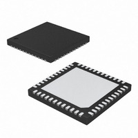
DS3514T+ Maxim Integrated Products, DS3514T+ Datasheet

DS3514T+
Specifications of DS3514T+
Related parts for DS3514T+
DS3514T+ Summary of contents
Page 1
... Analog Supply ♦ 2.7V to 5.5V Digital Supply ♦ 48-Pin TQFN Package (7mm x 7mm) C-compatible serial 2 C speeds up to PART DS3514T+ DS3514T+T&R + Denotes a lead-free/RoHS-compliant package. T&R = Tape and reel Exposed pad. Applications Buffer Pin Configuration and Typical Operating Circuit appear at Adjustment (Real end of data sheet ...
Page 2
I C Gamma and V ABSOLUTE MAXIMUM RATINGS Voltage Range on V Relative to GND ................-0.5V to +16V DD Voltage Range on VRL, VRH, GHH, GHM, GLM, GLL Relative to GND.........-0. 0.5V), not to exceed 16V ...
Page 3
I C Gamma and V INPUT ELECTRICAL CHARACTERISTICS (continued +2.7V to +5.5V -45°C to +95°C, unless otherwise noted PARAMETER SYMBOL Input Resistance (GHH, GHM, GLM, GLL) Input Resistance Tolerance Power-On Recall Voltage Power-Up ...
Page 4
I C Gamma and ELECTRICAL CHARACTERISTICS (V = +2.7V to +5.5V -45°C to +95°C, timing referenced PARAMETER SYMBOL SCL Clock Frequency Bus-Free Time between STOP and START Conditions Hold ...
Page 5
I C Gamma and V NONVOLATILE MEMORY CHARACTERISTICS ( +2.7V to +5.5V.) PARAMETER SYMBOL EEPROM Write Cycles Note 1: All voltages are referenced to ground. Currents entering the IC are specified positive and currents exiting the IC ...
Page 6
I C Gamma and S0/ GM1–G14 Figure 2. GM1–GM14 Settling Timing Diagram V S0/ GM1–GM14 Figure 3. ...
Page 7
I C Gamma and +5.0V +15V +25°C, unless otherwise noted DIGITAL SUPPLY STANDBY CURRENT vs SDA = SCL = ...
Page 8
I C Gamma and +5.0V +15V +25°C, unless otherwise noted INL 0.50 0.25 0 -0.25 -0.50 0 128 256 384 512 640 768 896 1024 GAMMA SETTING (DEC) ...
Page 9
I C Gamma and V PIN NAME TYPE 1–5, 9, 10, N.C. — Power DD 7 VRH Ref Input 8 VRL Ref Input 11, 18, 19, GND Power 21, 22 ...
Page 10
I C Gamma and V DS3514 SDA SCL I C INTERFACE A0 MODE0 BIT (CR.0) MODE1 BIT (CR.1) S0 LOGIC S1 AND S0/S1 PINS LD CONTROL S0/S1 BITS (SOFT S0/S1) LD VCAP COMPENSATION COMP V ...
Page 11
I C Gamma and V Detailed Description The DS3514 operates in one of three modes that deter- mine how the V and gamma DACs are COM controlled/updated. The first two modes allow “banked” control of the 14 gamma channels ...
Page 12
I C Gamma and V Map , the Latch A registers for each channel are accessed through memory addresses 00–1Ch. Then, like the other modes, the LD pin determines when the DACs are updated. If the LD signal is ...
Page 13
I C Gamma and V or exceeds +150°C. In this state, the V disabled (output goes high impedance) until the junc- tion temperature falls below +150°C. Slave Address Byte and Address Pin The slave address byte consists of a ...
Page 14
I C Gamma and V ADDRESS NAME (HEX) Latch A for GM13 Ch 1Ah, 1Bh Latch A for GM14 Ch 1Ch, 1Dh Reserved 1Eh–3Fh Soft S1/S0 40h Standby 41h Reserved 42h–47h Control 48h Reserved 49h Status Bits 4Ah Reserved ...
Page 15
I C Gamma and V Soft S0/S1 Register 40h: SOFT S1/S0 Bits FACTORY DEFAULT MEMORY TYPE 40h x x BIT 7 Bits 7:2 Reserved These bits are used when in SOFT S0/S1 Bit-Controlled Bank-Updating mode (MODE1 = 0, MODE0 ...
Page 16
I C Gamma and V Control Register 48h: Control Register (CR) FACTORY DEFAULT MEMORY TYPE 48h x x BIT 7 Bits 7:6 Reserved V and Gamma Bias Current Control Bits (BIAS[1:0]): COM 00 = 60% Bits 5 ...
Page 17
I C Gamma and Serial Interface Description The following terminology is commonly used data transfers. (See Figure 4 and the I describe I Electrical Characteristics for additional information.) Master device: The master ...
Page 18
I C Gamma and Communication Writing a single byte to a slave: The master must gen- erate a START condition, write the slave address byte (R/W = 0), write the memory address, write the byte ...
Page 19
I C Gamma and V 2 TYPICAL I C WRITE TRANSACTION MSB LSB START R/W READ/ SLAVE WRITE ADDRESS* 2 EXAMPLE I C TRANSACTIONS (WHEN A0 IS CONNECTED TO GND). C0h A) ...
Page 20
I C Gamma and MASTER Pin Configuration TOP VIEW GM14 37 GLM 38 GLL 39 GHM 40 GHH 41 GND 42 DS3514 ...
Page 21
... Maxim cannot assume responsibility for use of any circuitry other than circuitry entirely embodied in a Maxim product. No circuit patent licenses are implied. Maxim reserves the right to change the circuitry and specifications without notice at any time. Maxim Integrated Products, 120 San Gabriel Drive, Sunnyvale, CA 94086 408-737-7600 ____________________ 21 © 2008 Maxim Integrated Products ...


