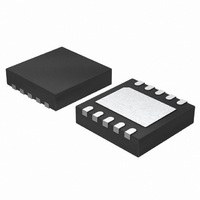
EL5228IL-T7A Intersil, EL5228IL-T7A Datasheet - Page 2

EL5228IL-T7A
Manufacturer Part Number
EL5228IL-T7A
Description
IC AMP VCOM DUAL BUFF 10-DFN
Manufacturer
Intersil
Specifications of EL5228IL-T7A
Applications
TFT-LCD Panels: Gamma Buffer, VCOM Driver
Number Of Circuits
2
-3db Bandwidth
12MHz
Slew Rate
10 V/µs
Current - Supply
3.5mA
Current - Output / Channel
120mA
Voltage - Supply, Single/dual (±)
4.5 V ~ 18 V
Mounting Type
Surface Mount
Package / Case
10-DFN
Lead Free Status / RoHS Status
Contains lead / RoHS non-compliant
Absolute Maximum Ratings
V
Supply Voltage between VSD and GND . . . . . . . . . . . . . . . . . . TBD
Maximum Continuous Output Current . . . . . . . . . . . . . . . . . . . . TBD
Ambient Operating Temperature . . . . . . . . . . . . . . . . . . . . . . . . TBD
CAUTION: Stresses above those listed in “Absolute Maximum Ratings” may cause permanent damage to the device. This is a stress only rating and operation of the
device at these or any other conditions above those indicated in the operational sections of this specification is not implied.
IMPORTANT NOTE: All parameters having Min/Max specifications are guaranteed. Typical values are for information purposes only. Unless otherwise noted, all tests
are at the specified temperature and are pulsed tests, therefore: T
Electrical Specifications
GAMMA BUFFER INPUT CHARACTERISTICS
V
TCV
I
R
C
A
GAMMA BUFFER OUTPUT CHARACTERISTICS
V
V
I
GAMMA BUFFER DYNAMIC PERFORMANCE
SR
t
BW
CS
V
V
TCV
I
R
C
CMIR
CMRR
A
V
V
V
I
I
CC
B
SC
S
B
SC
OUT
PARAMETER
V
VOL
OS
IN
IN
OL
OH
COM
OS
IN
IN
COM
OL
OH
OS
OS
Supply Voltage between VS and GND . . . . . . . . . . . . . . TBD
AMPLIFIER INPUT CHARACTERISTICS
AMPLIFIER OUTPUT CHARACTERISTICS
Input Offset Voltage
Average Offset Voltage Drift
Input Bias Current
Input Impedance
Input Capacitance
Voltage Gain
Output Swing Low
Output Swing High
Short Circuit Current
Slew Rate (Note 3)
Settling to +0.1%
-3dB Bandwidth
Channel Separation
Input Offset Voltage
Average Offset Voltage Drift (Note 4)
Input Bias Current
Input Impedance
Input Capacitance
Common-Mode Input Range
Common-Mode Rejection Ratio
Open-Loop Gain
Output Swing Low
Output Swing High
Short-circuit Current
Output Current
DESCRIPTION
2
V
S
(T
+ = +15V, V
A
= 25°C)
S
- = 0V, R
J
= T
L
V
(Note 1)
V
0.5 ≤ V
I
I
Short to GND (Note 2)
1V ≤ V
V
R
f = 5MHz
V
V
for V
0.5V ≤ V
I
I
C
= 1kΩ to 7.5V, T
L
L
L
L
CM
CM
O
CM
CM
L
= T
= -5mA
= 5mA
= -5mA
= 5mA
= 10kΩ, C
= 2V Step
= 7.5V
IN
A
= 7.5V
= 7.5V
= 7.5V
EL5228
OUT
OUT
from -0.5V to 15.5V
OUT
≤14V, 20% to 80%, R
≤ 14.5V, R
L
≤ 14.5V
= 10pF
CONDITION
Maximum Die Temperature . . . . . . . . . . . . . . . . . . . . . . . . . . . . TBD
Storage Temperature . . . . . . . . . . . . . . . . . . . . . . . . . . . . . . . . . TBD
Power Dissipation . . . . . . . . . . . . . . . . . . . . . . . . . . . . . See Curves
A
= 25°C unless otherwise specified.
L
= 10kΩ
L
= 10kΩ
0.995
14.85
14.85
MIN
-0.5
±80
53
62
7
14.92
14.92
±120
±180
TYP
500
±65
80
10
12
75
72
70
80
2
5
2
1
2
3
7
2
1
2
1.005
+15.5
MAX
150
150
14
50
15
60
µV/°C
µV/°C
UNIT
V/µs
MHz
V/V
mV
GΩ
mV
mA
mV
GΩ
mV
mA
mA
nA
pF
dB
nA
pF
dB
dB
ns
V
V
V


