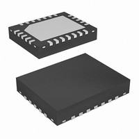
EL9201ILZ-T13 Intersil, EL9201ILZ-T13 Datasheet - Page 12

EL9201ILZ-T13
Manufacturer Part Number
EL9201ILZ-T13
Description
IC AMP VCOM PROGRAMMABLE 24-QFN
Manufacturer
Intersil
Datasheet
1.EL9200ILZ.pdf
(15 pages)
Specifications of EL9201ILZ-T13
Applications
TFT-LCD Panels: VCOM Driver
Output Type
Rail-to-Rail
Number Of Circuits
2
-3db Bandwidth
44MHz
Slew Rate
80 V/µs
Current - Supply
7.6mA
Current - Output / Channel
65mA
Voltage - Supply, Single/dual (±)
4.5 V ~ 16.5 V, ±2.25 V ~ 8.25 V
Mounting Type
Surface Mount
Package / Case
24-VQFN Exposed Pad, 24-HVQFN, 24-SQFN, 24-DHVQFN
Lead Free Status / RoHS Status
Lead free / RoHS Compliant
Non-Volatile Memory (EEPROM)
Programming
When the CTL pin exceeds 4.9V, the non-volatile
programming cycle will be activated. The CTL signal needs
to remain above 4.9V for more than 200µs. The level and
timing needed to program the non-volatile memory is given
below. It then takes a maximum of 100ms for the
programming to be completed inside the device (see P
specification in Table Electrical Specifications on page 3.
Amplifiers’ Operating Voltage, Input, and Output
The amplifiers are specified with a single nominal supply
voltage from 5V to 15V or a split supply with its total range
from 5V to 15V. Correct operation is guaranteed for a supply
range of 4.5V to 16.5V. Most amplifier specifications are
stable over both the full supply range and operating
temperatures of -40°C to +85°C. Parameter variations with
operating voltage and/or temperature are shown in the See
“Amplifier Typical Performance Curves” on page 6.
The input common-mode voltage range of the amplifiers
extends 500mV beyond the supply rails. The output swings
of the those typically extend to within 100mV of positive and
negative supply rails with load currents of 5mA. Decreasing
load currents will extend the output voltage range even
closer to the supply rails. Figure 27 shows the input and
output waveforms for the device in the unity-gain
configuration. Operation is from 5V supply with a 1kΩ load
connected to GND. The input is a 10V
output voltage is approximately 9.8V
FIGURE 29. OPERATION WITH RAIL-TO-RAIL INPUT AND
4.9V
CTL VOLTAGE
FIGURE 28. EEPROM PROGRAMMING
5V
5V
OUTPUT
CTL
12
PT
10µs
A
V
T
V
A
P-P
V
S
IN
= +25°C
P-P
= 1
= 5V
= 10V
.
sinusoid. The
P-P
EL9200, EL9201, EL9202
TIME
T
Short-Circuit Current Limit
The amplifiers will limit the short circuit current to ±180mA if
the output is directly shorted to the positive or the negative
supply. If an output is shorted indefinitely, the power
dissipation could easily increase such that the device may
be damaged. Maximum reliability is maintained if the output
continuous current never exceeds ±65mA. This limit is set by
the design of the internal metal interconnects.
Output Phase Reversal
The amplifiers are immune to phase reversal as long as the
input voltage is limited from V
Figure 28 shows a photo of the output of the device with the
input voltage driven beyond the supply rails. Although the
device's output will not change phase, the input's
overvoltage should be avoided. If an input voltage exceeds
supply voltage by more than 0.6V, electrostatic protection
diodes placed in the input stage of the device begin to
conduct and over-voltage damage could occur.
Unused Amplifiers
It is recommended that any unused amplifiers in a dual and
a quad package be configured as a unity gain follower. The
inverting input should be directly connected to the output
and the non-inverting input tied to the ground plane.
Power Supply Bypassing and Printed Circuit
Board Layout
The amplifiers can provide gain at high frequency. As with
any high-frequency device, good printed circuit board layout
is necessary for optimum performance. Ground plane
construction is highly recommended, lead lengths should be
as short as possible and the power supply pins must be well
bypassed to reduce the risk of oscillation. For normal
operation, a 0.1µF ceramic capacitor should be placed from
V
connected in parallel, placed in the region of the amplifier.
S
FIGURE 30. OPERATION WITH BEYOND-THE-RAILS INPUT
to pin to GND. A 4.7µF tantalum capacitor should then be
1V
1V
S
- -0.5V to V
10µs
V
A
T
V
A
S
V
IN
= +25°C
= 2.5V
= 1
= 6V
S
+ +0.5V.
P-P
October 30, 2008
FN7438.1


