AD532KH Analog Devices Inc, AD532KH Datasheet - Page 11
AD532KH
Manufacturer Part Number
AD532KH
Description
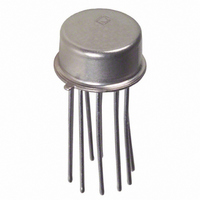
IC MULTIPLIER 10V TO-100-10
Manufacturer
Analog Devices Inc
Datasheet
1.AD532JD.pdf
(16 pages)
Specifications of AD532KH
Rohs Status
RoHS non-compliant
Function
Analog Multiplier/Divider
Number Of Bits/stages
4-Quadrant
Package / Case
TO-100, Metal Can (10 Leads)
No. Of Multipliers / Dividers
1
No. Of Amplifiers
3
Supply Voltage Range
± 10V To ± 18V
Slew Rate
45V/µs
Operating Temperature Range
0°C To +70°C
Digital Ic Case Style
TO-100
Lead Free Status / RoHS Status
Contains lead / RoHS non-compliant
Available stocks
Company
Part Number
Manufacturer
Quantity
Price

Part Number:
AD532KH
Manufacturer:
ADI/亚德诺
Quantity:
20 000


AD532 PERFORMANCE CHARACTERISTICS
Multiplication accuracy is defined in terms of total error at 25°C
with the rated power supply. The value specified is in percent of
full scale and includes X
scale factor error. To this must be added such application-
dependent error terms as power supply rejection, common-
mode rejection and temperature coefficients (although worst
case error over temperature is specified for the AD532S). Total
expected error is the rms sum of the individual components
because they are uncorrelated.
Accuracy in the divide mode is only a little more complex. To
achieve division, the multiplier cell must be connected in the
feedback of the output op amp as shown in Figure 17. In this
configuration, the multiplier cell varies the closed loop gain of
the op amp in an inverse relationship to the denominator voltage.
Therefore, as the denominator is reduced, output offset, band-
width, and other multiplier cell errors are adversely affected.
The divide error and drift are then ε
represents multiplier full-scale error and drift, and (X
the absolute value of the denominator.
NONLINEARITY
Nonlinearity is easily measured in percent harmonic distortion.
The curves of Figure 6 and Figure 7 characterize output distortion
as a function of input signal level and frequency respectively,
with one input held at plus or minus 10 V dc. In Figure 7, the
sine wave amplitude is 20 V (p-p).
AC FEEDTHROUGH
AC feedthrough is a measure of the multiplier’s zero suppression.
With one input at zero, the multiplier output should be zero
regardless of the signal applied to the other input. Feedthrough
as a function of frequency for the AD532 is shown in Figure 8.
It is measured for the condition V
V
consists primarily of the second harmonic and is measured in
millivolts peak-to-peak.
Y
= 0, V
X
= 20 V (p-p) over the given frequency range. It
IN
and Y
IN
X
nonlinearities, feedback and
= 0, V
m
× 10 V/X
Y
= 20 V (p-p) and
1
− X
2
) where ε
1
− X
2
) is
Rev. D | Page 11 of 16
m
COMMON-MODE REJECTION
The AD532 features differential X and Y inputs to enhance its
flexibility as a computational multiplier/divider. Common-mode
rejection for both inputs as a function of frequency is shown in
Figure 9. It is measured with X
10 V dc and Y
DYNAMIC CHARACTERISTICS
The closed loop frequency response of the AD532 in the multiplier
mode typically exhibits a 3 dB bandwidth of 1 MHz and rolls
off at 6 dB/octave, thereafter. Response through all inputs is
essentially the same as shown in Figure 10. In the divide mode,
the closed loop frequency response is a function of the absolute
value of the denominator voltage as shown in Figure 11.
Stable operation is maintained with capacitive loads to 1000 pF
in all modes, except the square root for which 50 pF is a safe
upper limit. Higher capacitive loads can be driven if a 100 Ω
resistor is connected in series with the output for isolation.
POWER SUPPLY CONSIDERATIONS
Although the AD532 is tested and specified with ±15 V dc supplies,
it may be operated at any supply voltage from ±10 V to ±18 V
for the J and K versions, and ±10 V to ±22 V for the S version.
The input and output signals must be reduced proportionately
to prevent saturation; however, with supply voltages below ±15 V,
as shown in Figure 12. Because power supply sensitivity is not
dependent on external null networks as in other conventionally
nulled multipliers, the power supply rejection ratios are improved
from 3 to 40 times in the AD532.
NOISE CHARACTERISTICS
All AD532s are screened on a sampling basis to assure that output
noise will have no appreciable effect on accuracy. Typical spot
noise vs. frequency is shown in Figure 13.
1
= Y
2
= 20 V (p-p), (X
1
= X
2
1
= 20 V (p-p), (Y
− X
2
) = 10 V dc.
1
AD532
− Y
2
) =
Related parts for AD532KH
Image
Part Number
Description
Manufacturer
Datasheet
Request
R

Part Number:
Description:
±1.7g Dual-Axis IMEMS Accelerometer Evaluation Board
Manufacturer:
Analog Devices Inc
Datasheet:

Part Number:
Description:
Inertial Sensor Evaluation System
Manufacturer:
Analog Devices Inc
Datasheet:
Part Number:
Description:
Manufacturer:
Analog Devices Inc
Datasheet:
Part Number:
Description:
Manufacturer:
Analog Devices Inc
Datasheet:
Part Number:
Description:
Manufacturer:
Analog Devices Inc
Datasheet:
Part Number:
Description:
Manufacturer:
Analog Devices Inc
Datasheet:
Part Number:
Description:
Manufacturer:
Analog Devices Inc
Datasheet:
Part Number:
Description:
Manufacturer:
Analog Devices Inc
Datasheet:
Part Number:
Description:
Manufacturer:
Analog Devices Inc
Datasheet:
Part Number:
Description:
Manufacturer:
Analog Devices Inc
Datasheet:
Part Number:
Description:
Manufacturer:
Analog Devices Inc
Datasheet:
Part Number:
Description:
Manufacturer:
Analog Devices Inc
Datasheet:
Part Number:
Description:
Manufacturer:
Analog Devices Inc
Datasheet: