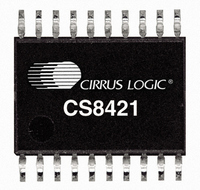
CS8421-CNZ Cirrus Logic Inc, CS8421-CNZ Datasheet - Page 22

CS8421-CNZ
Manufacturer Part Number
CS8421-CNZ
Description
IC SAMPLE RATE CONVERTER 20QFN
Manufacturer
Cirrus Logic Inc
Type
Sample Rate Converterr
Datasheet
1.CS8421-CZZ.pdf
(36 pages)
Specifications of CS8421-CNZ
Package / Case
20-QFN
Applications
Digital Audio
Mounting Type
Surface Mount
Operating Supply Voltage
3.3 V / 5.0 V
Operating Temperature Range
- 10 C to + 70 C
Mounting Style
SMD/SMT
Lead Free Status / RoHS Status
Lead free / RoHS Compliant
For Use With
598-1018 - BOARD EVAL FOR CS8421
Lead Free Status / Rohs Status
Lead free / RoHS Compliant
Other names
598-1730
Available stocks
Company
Part Number
Manufacturer
Quantity
Price
Company:
Part Number:
CS8421-CNZ
Manufacturer:
CIRRUS
Quantity:
235
22
4.3.7
4.4
SDOUT/
TDM_IN
OLRCK
OSCLK
Time Division Multiplexing (TDM) Mode
TDM Mode allows several CS8421 to be serially connected together allowing their corresponding SDOUT
data to be multiplexed onto one line for input into a DSP or other TDM-capable multichannel device.
The CS8421 can operate in two TDM modes. The first mode consists of all of the CS8421’s output ports set
to slave, as shown in
the remaining CS8421’s output ports set to slave, as shown in
The TDM_IN pin is used to input the data, while the SDOUT pin is used to output the data. The first CS8421
in the chain should have its TDM_IN set to GND. Data is transmitted from SDOUT most significant bit first
on the first OSCLK falling edge after an OLRCK transition and is valid on the rising edge of OSCLK.
In TDM Slave Mode, the number of channels that can by multiplexed to one serial data line depends on the
output sampling rate. For Slave Mode, OSCLK must operate at N*64*Fso, where N is the number of
CS8421’s connected together. The maximum allowable OSCLK frequency is 24.576 MHz, so for Fso =
48 kHz, N = 8 (16 channels of serial audio data).
In TDM Master Mode, OSCLK operates at 256*Fso, which is equivalent to N = 4, so a maximum of 8 chan-
nels of digital audio can be multiplexed together. Note that for TDM Master Mode, MCLK must be at least
256*Fso, where Fso 96 kHz. OLRCK identifies the start of a new frame. Each time-slot is 32-bits wide,
with the valid data sample left-justified within the time-slot. Valid data lengths are 16-, 20-, 24- or 32-bits.
Figures 11
• If the input is set to master, Fsi XTI/128 and Fso XTI/130.
• If the output is set to master, Fso XTI/128 and Fsi XTI/130.
• If both input and output are set to slave, XTI 130*[maximum(Fsi,Fso)], XTI/Fsi < 3750, and XTI/Fso <
Clocking
In order to ensure proper operation of the CS8421, the clock or crystal attached to XTI must simultaneous-
ly satisfy the requirements of LRCK for both the input and output as follows:
3750.
MSB
SDOUT 4, ch A
32 clks
and
12
LSB
show the interface format for Master and Slave TDM Modes with a 32-bit word-length.
MSB
SDOUT 4, ch B
Figure 10. Typical Connection Diagram for Crystal Circuit
Figure
32 clks
Figure 11. TDM Slave Mode Timing Diagram
LSB
13. The second mode consists of one CS8421 output port set to master and
MSB
SDOUT 3, ch A
32 clks
XTI
C
LSB
MSB
SDOUT 3, ch B
32 clks
LSB
MSB
SDOUT 2, ch A
XTO
32 clks
R
C
Figure
LSB
MSB
14.
SDOUT 2, ch B
32 clks
LSB
MSB
SDOUT 1, ch A
32 clks
LSB
MSB
SDOUT 1, ch B
CS8421
32 clks
DS641F5
LSB


