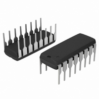
SA572NG ON Semiconductor, SA572NG Datasheet - Page 7

SA572NG
Manufacturer Part Number
SA572NG
Description
IC COMPANDOR 2CHAN GAIN 16-DIP
Manufacturer
ON Semiconductor
Type
Compandorr
Datasheet
1.SA572DTBR2.pdf
(12 pages)
Specifications of SA572NG
Applications
Automatic Level Control, Stereo Expander
Mounting Type
Through Hole
Package / Case
16-DIP (0.300", 7.62mm)
Maximum Operating Temperature
+ 85 C
Mounting Style
Through Hole
Minimum Operating Temperature
- 40 C
Lead Free Status / RoHS Status
Lead free / RoHS Compliant
Other names
SA572NG
SA572NGOS
SA572NGOS
Available stocks
Company
Part Number
Manufacturer
Quantity
Price
Part Number:
SA572NG
Manufacturer:
ON/安森美
Quantity:
20 000
Basic Expandor
expandor. The gain expression of the system is given by:
nodes. R
current into the gain cell can be as large as 140 mA. This
corresponds to a voltage level of 140 mA•6.8 kW = 952 mV
peak. The input peak current into the rectifier is limited to
300 mA by the internal bias system. Note that the value of
R
and R
R
small R
static and dynamic tracking error. However, an impedance
Basic Compressor
compressor. The IC is put in the feedback loop of the OPA
A
1
3
1
Figure 6 shows an application of the circuit as a simple
Both the resistors R
Figure 7 shows the hook-up of the circuit as a
/R
. The system gain expression is as follows:
can be increased to accommodate higher input level. R
V
2
3
IN
for desirable system voltage and current levels. A
are external resistors. It is easy to adjust the ratio of
2
1
results in higher gain control current and smaller
is a 6.8 kW internal resistor. The maximum input
C
2.2mF
IN1
V
V
V
V
OUT
OUT
IN
IN
+
+
R
100kW
1
5
(I
(I
and R
1
1
I
2
I
2
1
1
= 140 mA)
= 140 mA)
−
+
@
@
A1
2
R
R
are tied to internal summing
3
3
R
R
@ V
@ V
2
2
@ R
@ R
IN(AVG)
IN(AVG)
1
1
Figure 6. Basic Expandor Schematic
2.2mF
C
3.3kW
2
C
2.2mF
1
2
IN3
R
IN2
2
(3,13)
(7,9)
(8)
6.8kW
http://onsemi.com
R
(eq. 4)
(eq. 6)
1
2
BUFFER
DG
7
(16)
buffer A
with large source impedance.
the external OPA A
current to the output voltage. In high-performance
applications, A
band so that the high-performance output of the gain cell
will not be degraded. The non-inverting input of A
biased at the low noise internal reference Pin 6 or 10.
Resistor R
maximum swing. The output DC level of A
supply system and be grounded for a single supply system.
C
time constant.
output DC level of A
overload protection.
V
A
REF
The gain cell output current feeds the summing node of
V
R
The zener diodes D
DC1
B
sets the attack time constant and C
+V
can be tied to a regulated power supply for a dual
CC
+VB
(6,10)
(4,12)
(5,11)
(2,14)
, R
1
V
V
C
1kW
1mF
may be necessary if the input is voltage driven
4
DC2
OUT
OUT
A
R
is used to bias up the output DC level of A
6
R
4
10mF
C
, and CDC form a DC feedback for A
DC + V
DC + V
R
2
has to be low-noise, high-speed and wide
2
* V
. R
C
2.2mF
1
1
3
is given by:
B
REF
REF
1
and A
@
A2
and D
17.3kW
R
R
1 )
1 )
3
DC1
2
convert the gain cell output
2
R
) R
R
R
R
4
DC1
3
4
are used for channel
DC2
* V
R
R
) R
sets the recovery
4
B
2
DC2
is given by:
R
R
3
4
V
OUT
2
can be
1
(eq. 7)
(eq. 5)
. The
2
for


