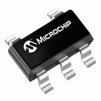
MCP6541T-E/OT Microchip Technology, MCP6541T-E/OT Datasheet - Page 16

MCP6541T-E/OT
Manufacturer Part Number
MCP6541T-E/OT
Description
IC COMP 1.6V SNGL P-P SOT23-5
Manufacturer
Microchip Technology
Type
General Purposer
Datasheets
1.MCP6541T-ILT.pdf
(34 pages)
2.MCP6544-IST.pdf
(28 pages)
3.MCP6541T-EOT.pdf
(34 pages)
4.MCP6541T-EOT.pdf
(28 pages)
Specifications of MCP6541T-E/OT
Output Type
CMOS, Push-Pull, Rail-to-Rail, TTL
Package / Case
SC-74A, SOT-753
Number Of Elements
1
Voltage - Supply
1.6 V ~ 5.5 V
Mounting Type
Surface Mount
Number Of Channels
1 Channel
Product
Analog Comparators
Offset Voltage (max)
7 mV
Input Bias Current (max)
0.000001 uA
Supply Voltage (max)
5.5 V
Supply Voltage (min)
1.6 V
Maximum Operating Temperature
+ 125 C
Mounting Style
SMD/SMT
Minimum Operating Temperature
- 40 C
Comparator Type
Low Power
No. Of Comparators
1
Response Time
4µs
Ic Output Type
CMOS, Push Pull, TTL
Supply Current
600nA
Supply Voltage Range
1.6V To 5.5V
Amplifier Case Style
SOT-23
Rohs Compliant
Yes
Output Compatibility
CMOS, TTL
Lead Free Status / RoHS Status
Lead free / RoHS Compliant
Lead Free Status / RoHS Status
Lead free / RoHS Compliant, Lead free / RoHS Compliant
Other names
MCP6541T-E/OT
MCP6541T-E/OTTR
MCP6541T-E/OTTR
Available stocks
Company
Part Number
Manufacturer
Quantity
Price
MCP6541/1R/1U/2/3/4
4.4.2
Figure 4-6
using three resistors. The resulting hysteresis diagram
is shown in
FIGURE 4-6:
Hysteresis.
FIGURE 4-7:
Inverting Circuit.
In order to determine the trip voltages (V
for the circuit shown in
simplified to the Thevenin equivalent circuit with
respect to V
FIGURE 4-8:
DS21696F-page 16
V
V
V
V
OH
DD
OL
SS
V
V
23
SS
V
IN
R
R
Low-to-High
V
2
3
OUT
shows an inverting circuit for single-supply
V
INVERTING CIRCUIT
Figure
DD
DD
, as shown in
R
23
4-7.
V
MCP654X
TLH
Inverting Circuit With
Hysteresis Diagram for the
Thevenin Equivalent Circuit.
Figure
V
+
-
MCP654X
DD
V
THL
V
Figure
DD
R
4-6, R
F
High-to-Low
V
R
SS
F
4-8.
2
and R
THL
V
V
DD
OUT
and V
V
3
OUT
can be
V
IN
TLH
)
Where:
Using this simplified circuit, the trip voltage can be
calculated using the following equation:
EQUATION 4-2:
Figure 2-20
typical values for V
4.5
With this family of comparators, the power supply pin
(V
capacitor (i.e., 0.01 µF to 0.1 µF) within 2 mm for good
edge rate performance.
4.6
Reasonable capacitive loads (e.g., logic gates) have
little impact on propagation delay (see
The supply current increases with increasing toggle
frequency
capacitive loads.
4.7
In order to maximize battery life in portable
applications, use large resistors and small capacitive
loads. Avoid toggling the output more than necessary.
Do not use Chip Select (CS) frequently to conserve
start-up power. Capacitive loads will draw additional
power at start-up.
V
V
DD
TLH
THL
for single supply) should have a local bypass
V
= trip voltage from low to high
= trip voltage from high to low
V
THL
TLH
Bypass Capacitors
Capacitive Loads
Battery Life
and
(Figure
=
=
V
V
V
Figure 2-23
OH
OL
23
OH
⎛
⎜
⎝
⎛
⎜
⎝
R
2-19),
---------------------- -
R
---------------------- -
R
=
23
23
and V
23
R
R
------------------
R
© 2007 Microchip Technology Inc.
=
+
+
23
2
23
R
+
R F
R F
------------------
R
3
R
OL
2
R
can be used to determine
especially
⎞
⎟
⎠
2
⎞
⎟
⎠
+
3
R
.
+
+
×
R
3
3
V
V
V
23
DD
23
⎛
⎝
⎛
⎝
--------------------- -
R
--------------------- -
R
23
23
R
R
Figure
with
+
+
F
F
R
R
F
F
⎞
⎠
⎞
⎠
higher
2-31).


