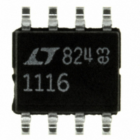
LT1116CS8#PBF Linear Technology, LT1116CS8#PBF Datasheet - Page 3

LT1116CS8#PBF
Manufacturer Part Number
LT1116CS8#PBF
Description
IC COMPARATOR 12NS SINGLE 8SOIC
Manufacturer
Linear Technology
Series
UltraFast™r
Type
General Purposer
Datasheet
1.LT1116CN8PBF.pdf
(8 pages)
Specifications of LT1116CS8#PBF
Number Of Elements
1
Output Type
CMOS, Complementary, TTL
Mounting Type
Surface Mount
Package / Case
8-SOIC (0.154", 3.90mm Width)
Comparator Type
High Speed
No. Of Comparators
1
Response Time
10ns
Ic Output Type
CMOS, MOS, Open-Collector / Drain, TTL
Supply Current
27mA
Rohs Compliant
Yes
Lead Free Status / RoHS Status
Lead free / RoHS Compliant
Available stocks
Company
Part Number
Manufacturer
Quantity
Price
ELECTRICAL CHARACTERISTICS
range, otherwise specifications are at T
SYMBOL
V
V
I
t
t
∆t
t
t
Note 1: Stresses beyond those listed under Absolute Maximum Ratings
may cause permanent damage to the device. Exposure to any Absolute
Maximum Rating condition for extended periods may affect device
reliabilty and lifetime.
Note 2: Input offset voltage is defined as the average of two offset
voltages measured by forcing first the Q output to 1.4V then forcing
the Q output to 1.4V.
Note 3: Input bias current is defined as the average of the two input
currents.
TYPICAL PERFOR A CE CHARACTERISTICS
IL
PD
PD
SU
H
IH
IL
PD
5.0
4.5
4.0
3.5
3.0
2.5
2.0
1.5
1.0
0.5
0
–2.5
Gain CharacteristIcs
T
J
= 125°C
T
DIFFERENTIAL INPUT VOLTAGE (mV)
J
–1.5
= –55°C
PARAMETERS
+ Positive Latch Threshold
– Latch Threshold
Latch Input Current
Propagation Delay
Propagation Delay
Differential Propagation Delay
Latch Set-Up Time
Latch Hold Time
– 0.5
0
0.5
T
J
= 25°C
W
1.5
V
I
OUT
LT1116 • TPC01
S
= ±5V
= 0
U
2.5
A
= 25°C. V
CONDITIONS
V
∆V
∆V
∆V
(Note 5)
(Note 5)
LATCH
IN
IN
IN
25
20
10
15
= 100mV, OD = 5mV (Note 4)
= 100mV, OD = 20mV (Note 4)
= 100mV, OD = 5mV (Note 4)
+
5
0
= 0V
= 5V, V
0
Propagation Delay vs Overdrive
T
STEP SIZE = 100mV
J
= 25°C
t
PDHL
t
The
PDLH
10
+
OVERDRIVE VOLTAGE (mV)
= –5V, V
●
denotes the specifications which apply over full operating temperature
20
Note 4: t
equipment with low values of overdrive. The LT1116 is sample tested with
a 1V step and 500mV overdrive. Correlation tests have shown that t
∆t
to verify internal bias conditions are correct. For low overdrive conditions
V
Note 5: Input latch set-up time, t
must be stable prior to asserting the latch signal. The hold time,
t
be stable.
OUT
H
OS
, is the interval after the latch is asserted in which the input signal must
PD
30
is added to the measured overdrive.
= (Q) = I .4V, LATCH = 0V, unless noted.
can be guaranteed with this test if additional DC tests are performed
PD
40
and ∆t
LT1116 • TPC02
●
●
●
●
●
PD
50
cannot be measured in automatic handling
MIN
2.0
20
18
16
14
12
10
6
4
2
8
0
SU
0
Propagation Delay
vs Load Capacitance
STEP = 100mV, OVERDRIVE = 5mV
, is the interval in which the input signal
TYP
–20
12
10
2
2
OUTPUT LOAD CAPACITANCE (pF)
10
MAX
–500
0.8
16
14
20
18
16
3
t
PDHL
30
LT1116
t
PDLH
40
LT1116 • TPC03
UNITS
PD
1116fb
3
and
µA
ns
ns
ns
ns
ns
ns
ns
50
V
V


