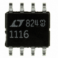
LT1116CS8#PBF Linear Technology, LT1116CS8#PBF Datasheet - Page 6

LT1116CS8#PBF
Manufacturer Part Number
LT1116CS8#PBF
Description
IC COMPARATOR 12NS SINGLE 8SOIC
Manufacturer
Linear Technology
Series
UltraFast™r
Type
General Purposer
Datasheet
1.LT1116CN8PBF.pdf
(8 pages)
Specifications of LT1116CS8#PBF
Number Of Elements
1
Output Type
CMOS, Complementary, TTL
Mounting Type
Surface Mount
Package / Case
8-SOIC (0.154", 3.90mm Width)
Comparator Type
High Speed
No. Of Comparators
1
Response Time
10ns
Ic Output Type
CMOS, MOS, Open-Collector / Drain, TTL
Supply Current
27mA
Rohs Compliant
Yes
Lead Free Status / RoHS Status
Lead free / RoHS Compliant
Available stocks
Company
Part Number
Manufacturer
Quantity
Price
LT1116
APPLICATIO S I FOR ATIO
Common Mode Considerations
The LT1116 is specified for a common mode range of 0V
to 2.5V with a single 5V supply, and –5V to 2.5V with ±5V
supplies. The common mode range is defined as the DC
input for which the output responds correctly to small
changes in the input differential. Input signals can exceed
the positive common mode limit up to the 15V absolute
maximum rating without damaging the comparator. There
will, however, be an increase in propagation delay of up to
10ns when the input signal switches back into the
common mode range. When input signals fall below the
negative common mode limit, the internal PN diode formed
with the substrate can turn on (resulting in significant
charge flow throughout the die). A Schottky clamp diode,
between the input and the negative rail, speeds up recov-
ery from negative overdrive by preventing the substrate
diode from turning on. The zero crossing detector in
Figure 1 demonstrates the use of a fast clamp diode.
Recovery, from 500mV overdrive below V
is approximately 18ns.
Input Characteristics
Each input to the LT1116 is buffered with a fast PNP
follower—input bias current therefore does not vary
significantly throughout the common mode range. When
either input exceeds the positive common mode limit, the
bias current drops to zero. Inputs that fall more than one
diode and drop below V
clamp diode, causing large input current to flow.
Figure 1. The Zero Crossing Detector Terminates the
Transmission Line At Its 50Ω Characteristic Impedance. Negative
Inputs Should Not Fall Below –2V to keep the Signal Current
Within the Clamp Diode’s Maximum Forward Rating. Positive
Inputs Should not Exceed the Devices Absolute Maximum Ratings
nor the Power Rating on the Terminating Resistor
6
V
IN
50Ω
R
S
CABLE
Fast Zero Crossing Detector
U
–
will forward bias the substrate or
U
1N5712
W
R
50Ω
T
–
, for this circuit
+
–
LT1116
U
5V
LT1116 • AI01
Q
–
Q
Single ended input resistance is about 5MΩ, and remains
roughly constant over the input common mode range. The
common mode resistance is about 2.5MΩ with zero
differential input voltage, and does not change
significantly with the absolute value of differential input.
Effective input capacitance, typically 5pF, is determined by
measuring the resulting change in propagation delay for a
1kΩ change in source resistance.
Latch Pin Dynamics
The internal latch uses local regenerative feedback to
shorten set-up and hold times. Driving the latch pin high
retains the output state. The latch pin floats to a high state
when disconnected, so it must be driven low for
flow-through operation. The set-up time required to
guarantee detecting a given transition of the inputs is 2ns.
The inputs must also remain stable for a 2ns hold time
after latch is asserted. New data will appear at the output
approximately 10ns to 12ns after the latch goes low. The
latch pin has no built-in hysteresis, and is designed to be
driven from TTL or CMOS logic gates.
Additional Information
Linear Technology’s Application Note 13 provides an
extensive discussion of design techniques for high speed
comparators.
Figure 2. This Single Supply Crystal Oscillator Utilizes Crystals
From 10MHz To 15MHz Without Component Changes
5V
Single Supply Crystal Oscillator 10MHZ to 15MHz
1kΩ
1kΩ
24pF
10 TO 15MHz
AT CUT
2kΩ
+
–
LT1116
5V
Q
Q
–
LT1116 • AI02
OUTPUT
1116fb


