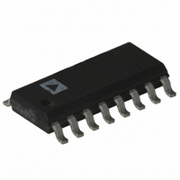
AD96685BRZ Analog Devices Inc, AD96685BRZ Datasheet - Page 2

AD96685BRZ
Manufacturer Part Number
AD96685BRZ
Description
IC COMP SNGL ULTRA-FAST 16-SOIC
Manufacturer
Analog Devices Inc
Type
with Latchr
Datasheet
1.AD96687BRZ.pdf
(8 pages)
Specifications of AD96685BRZ
Number Of Elements
1
Output Type
Complementary, ECL, Open-Emitter
Mounting Type
Surface Mount
Package / Case
16-SOIC (0.154", 3.90mm Width)
Number Of Elements
1
Input Offset Voltage
2@5/-5.2VmV
Input Bias Current (typ)
10uA
Response Time
2ns
Single Supply Voltage (typ)
Not RequiredV
Dual Supply Voltage (typ)
5/-5.2V
Supply Current (max)
9mA
Common Mode Rejection Ratio
90dB
Power Supply Rejection Ratio
70dB
Power Supply Requirement
Dual
Single Supply Voltage (min)
Not RequiredV
Single Supply Voltage (max)
Not RequiredV
Dual Supply Voltage (max)
±6.5V
Operating Temp Range
-25C to 85C
Operating Temperature Classification
Commercial
Mounting
Surface Mount
Pin Count
16
Package Type
SOIC N
Comparator Type
High Speed
No. Of Comparators
1
Ic Output Type
Open Emitter
Supply Current
9mA
Supply Voltage Range
5V, -5.2V
Amplifier Case Style
SOIC
Rohs Compliant
Yes
Lead Free Status / RoHS Status
Lead free / RoHS Compliant
Available stocks
Company
Part Number
Manufacturer
Quantity
Price
Part Number:
AD96685BRZ-REEL
Manufacturer:
ADI/亚德诺
Quantity:
20 000
AD96685/AD96687–SPECIFICATIONS
ELECTRICAL CHARACTERISTICS
Parameter
INPUT CHARACTERISTICS
ENABLE INPUT
DIGITAL OUTPUTS
SWITCHING PERFORMANCES
POWER SUPPLY
NOTES
1
2
3
4
5
6
7
Specifications subject to change without notice.
R
Input Voltage Range can be extended to –3.3 V if –V
Outputs terminated through 50 Ω to –2.0 V.
Propagation delays measured with 100 mV pulse (10 mV overdrive) to 50% transition point of the output.
Change in propagation delay from 100 mV to 1 V input overdrive.
Supply voltages should remain stable within ± 5% for normal operation.
Measured at ± 5% of +V
S
Input Offset Voltage
Input Offset Drift
Input Bias Current
Input Offset Current
Input Resistance
Input Capacitance
Input Voltage Ranges
Common-Mode Rejection Ratio
Logic “1” Voltage
Logic “0” Voltage
Logic “1” Current
Logic “0” Current
Logic “1” Voltage
Logic “0” Voltage
Propagation Delays
Dispersions
Latch Enable
Positive Supply Current (+5.0 V)
Negative Supply Current (–5.2 V)
Power Supply Rejection Ratio
= 100 Ω.
Input to Output HIGH
Input to Output LOW
Latch Enable to Output HIGH
Latch Enable to Output LOW
Minimum Pulsewidth
Minimum Setup Time
Minimum Hold Time
5
DIFFERENTIAL
6
S
VOLTAGE
ENABLE
and –V
4
3
LATCH
INPUT
2
S
Q
Q
.
COMPARE
LATCH
7
V
IN
S
V
Temp
25°C
Full
Full
25°C
Full
25°C
Full
25°C
25°C
Full
Full
Full
Full
Full
Full
Full
Full
25°C
25°C
25°C
25°C
25°C
25°C
25°C
25°C
Full
Full
Full
t
= –6.0 V.
DD
S
t
PD
t
H
(Positive Supply Voltage = 5.0 V; Negative Supply Voltage = –5.2 V, unless otherwise noted.)
Level
Test
VI
VI
VI
VI
VI
VI
VI
VI
VI
VI
VI
IV
IV
IV
IV
IV
IV
IV
VI
VI
VI
V
V
V
V
I
I
I
t
PW
t
PD
(E)
(E)
Min
–2.5
–1.1
–1.1
80
60
Industrial Temperature Range –25 C to +85 C
AD96685BR
50%
50%
50%
V
OS
Typ
1
20
7
0.1
200
2
2.5
2.5
2.5
2.5
50
2.0
0.5
0.5
70
90
8
15
Max
2
3
10
13
1.0
1.2
+5.0
–1.5
40
5
–1.5
3.5
3.5
3.5
3.5
3.0
1.0
1.0
9
18
t
t
t
t
t
V
V
PD
PD
PW
S
H
OS
OD
(E)
(E)
– Minimum Setup Time
– Minimum Hold Time
– Input to Output Delay
– LATCH ENABLE to Output Delay
– Minimum LATCH ENABLE Pulsewidth
– Input Offset Voltage
– Overdrive Voltage
Min
–2.5
80
–1.1
–1.1
60
AD96687BQ/BP/BR
Typ
1
20
7
0.1
200
2
90
2.5
2.5
2.5
2.5
50
2.0
0.5
0.5
15
31
70
Max
2
3
10
13
1.0
1.2
+5.0
–1.5
40
5
–1.5
3.5
3.5
3.5
3.5
3.0
1.0
1.0
18
36
Unit
mV
mV
µV/°C
µA
µA
µA
µA
kΩ
pF
V
dB
V
V
µA
µA
V
V
ns
ns
ns
ns
ps
ns
ns
ns
mA
mA
dB


