ISL45042IRZ Intersil, ISL45042IRZ Datasheet
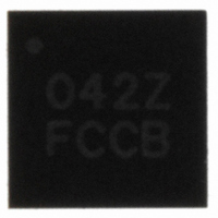
IC CALIBRATOR LCD MODULE 8-DFN

ISL45042IRZ

Manufacturer Part Number
ISL45042IRZ
Description
IC CALIBRATOR LCD MODULE 8-DFN
Manufacturer
Intersil
Type
Calibratorr
Datasheet

Specifications of ISL45042IRZ

Applications
LCD Display
Mounting Type
Surface Mount
Package / Case
8-TDFN
Lead Free Status / RoHS Status
Lead free / RoHS Compliant
LCD Module Calibrator
The V
remove flicker. The ISL45042 can be used to digitally adjust
a panel’s V
The output of the ISL45042 is connected to an external
voltage divider and an external V
application, the user can control the V
accuracy (128 steps). Once the desired V
obtained, the settings can be stored in the non-volatile
EEPROM memory, which would then be automatically
recalled during every power-up.
The V
programming is through a single interface pin (CTL). Once
the desired programmed value is obtained, the Counter
Enable pin (CE) can be used to prevent further adjustment
or programming.
The full-scale sink current of the ISL45042 is set using an
external resistor connected to the SET pin. The full-scale
sink current determines the lowest voltage of the external
voltage divider.
The ISL45042 is available in an 8 Ld 3mmx3mm TDFN
package with a maximum thickness of 0.8mm for ultra thin
LCD panel design.
Pinout
COM
COM
COM
voltage of an LCD panel needs to be adjusted to
adjustment and non-volatile memory
AVDD
voltage by controlling its output sink current.
GND
OUT
DNC
1
2
3
4
(8 LD TDFN)
TOP VIEW
ISL45042
1
COM
Data Sheet
COM
8
7
6
5
buffer amplifier. In this
1-888-INTERSIL or 1-888-468-3774
SET
CE
CTL
V
COM
DD
voltage with 7-bit
setting is
CAUTION: These devices are sensitive to electrostatic discharge; follow proper IC Handling Procedures.
|
Intersil (and design) is a trademark owned by Intersil Corporation or one of its subsidiaries.
Features
• 128-Step Adjustable Sink Current Output
• 2.6V to 3.6V Digital Supply Voltage Operating Range
• 4.5V to 20V Analog Supply Voltage Operating Range
• Rewritable EEPROM for Storing the Optimum V
• Output Adjustment Enable/Disable Control
• Output Guaranteed Monotonic Over-Temperature
• Two Pin Adjustment, Programming and Enable
• Ultra Thin 8 Ld 3mmx3mm DFN (0.8mm Max)
• Pb-Free (RoHS Compliant)
Applications
• LCD Panels
Ordering Information
NOTES:
ISL45042IRZ
1. Add “-T*” suffix for tape and reel. Please refer to
2. These Intersil Pb-free plastic packaged products employ special Pb-
3. For Moisture Sensitivity Level (MSL), please see device information
PART NUMBER
(3.0V Minimum Programming Voltage)
(10.8V Minimum Programming Voltage)
(Notes 1, 2, 3)
reel specifications.
free material sets, molding compounds/die attach materials, and
100% matte tin plate plus anneal (e3 termination finish, which is
RoHS compliant and compatible with both SnPb and Pb-free
soldering operations). Intersil Pb-free products are MSL classified at
Pb-free peak reflow temperatures that meet or exceed the Pb-free
requirements of IPC/JEDEC J STD-020.
page for ISL45042. For more information on MSL please see
techbrief TB363.
All other trademarks mentioned are the property of their respective owners.
April 13, 2011
Copyright © Intersil Americas Inc. 2005-2008, 2011. All Rights Reserved.
MARKING
042Z
PART
-40 to +85 8 Ld 3x3 TDFN
RANGE
TEMP.
(°C)
ISL45042
PACKAGE
(Pb-Free)
TB347
FN6072.9
COM
for details on
Value
L8.3x3A
DWG. #
PKG.

Related parts for ISL45042IRZ

ISL45042IRZ Summary of contents

Page 1

... Pb-Free (RoHS Compliant) Applications • LCD Panels Ordering Information PART NUMBER (Notes ISL45042IRZ NOTES: 1. Add “-T*” suffix for tape and reel. Please refer to reel specifications. 2. These Intersil Pb-free plastic packaged products employ special Pb- free material sets, molding compounds/die attach materials, and ...

Page 2

Pin Descriptions PIN OUT Adjustable Sink Current Output Pin. The current sinks into the OUT pin is equal to the DAC setting times the maximum adjustable sink current divided by 128. See SET pin function in “Pin Descriptions” on page ...

Page 3

... Moisture Sensitivity (see Technical Brief TB363) All Packages . . . . . . . . . . . . . . . . . . . . . . . . . . . . . . . . . . . Level 1 Maximum Junction Temperature (Plastic Package +150°C Maximum Storage Temperature Range . . . . . . . . . .-65°C to +150°C Pb-free Reflow Profile . . . . . . . . . . . . . . . . . . . . . . . . .see link below http://www.intersil.com/pbfree/Pb-FreeReflow.asp Erase/Write Cycles . . . . . . . . . . . . . . . . . . . . . . . . . . . . . . . . 10,000 Data Retention years @ +85° 18V 5kΩ 10kΩ 10kΩ; Unless Otherwise Specified. ...

Page 4

Electrical Specifications Test Conditions: V Typicals are at T PARAMETER CTL EEPROM Program Voltage CTL CTL EEPROM Programming Signal Time Programming Time SET Voltage Resolution SET Differential Nonlinearity SET Zero-Scale Error SET Full-Scale Error SET Current SET External Resistance AVDD ...

Page 5

AVDD ISL45042 I SINK CTL CE OUT SET R SET + - COLUMN DRIVER SINGLE PIXEL IN LCD PANEL FIGURE 1. VCOM ADJUSTMENT IN AN LCD PANEL Application Information The application circuit to adjust the V COM panel is shown ...

Page 6

Expected Output Voltage The ISL45042 provides an output sink current, which lowers the voltage on the external voltage divider (V voltage). Equations 1 and 2 can be used to calculate the output current (I ) and output voltage (V OUT ...

Page 7

Power Supply Sequence The recommended power supply sequencing is shown in Figure 6. When applying power, VDD should be applied before or at the same time as AVDD. The minimum time for t is 0µs. When removing power, the sequence ...

Page 8

... Accordingly, the reader is cautioned to verify that data sheets are current before placing orders. Information furnished by Intersil is believed to be accurate and reliable. However, no responsibility is assumed by Intersil or its subsidiaries for its use; nor for any infringements of patents or other rights of third parties which may result from its use ...

Page 9

Package Outline Drawing L8.3x3A 8 LEAD THIN DUAL FLAT NO-LEAD PLASTIC PACKAGE Rev 4, 2/10 3.00 6 PIN 1 INDEX AREA (4X) 0.15 TOP VIEW 2X 1.950 PIN #1 1 INDEX AREA 0.30 ± 0.10 2.30 ±0.10 ...

Related keywords