LMH0307GRE/NOPB National Semiconductor, LMH0307GRE/NOPB Datasheet - Page 10
LMH0307GRE/NOPB
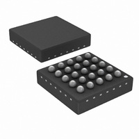
Manufacturer Part Number
LMH0307GRE/NOPB
Description
IC CBL DVR DUAL HD/SD 25-UARRAY
Manufacturer
National Semiconductor
Type
Driverr
Datasheet
1.LMH0307GRENOPB.pdf
(16 pages)
Specifications of LMH0307GRE/NOPB
Applications
Amplifiers, Video Distribution
Mounting Type
Surface Mount
Package / Case
25-Micro Array
Lead Free Status / RoHS Status
Lead free / RoHS Compliant
Other names
LMH0307GRETR


www.national.com
Address R/W Name
00h
01h
02h
R/W ID
R/W MASK
R
STATUS
Bits Field
7:1
7:5
0
4
3
2
1
0
7
6
5
4
3
2
1
0
DEVID
RSVD
RSVD
TF1N
TF1P
TF0N
TF0P
LOS
SD
PD1
PD0
MTF1N
MTF1P
MTF0N
MTF0P
MLOS
TABLE 1. SMBus Registers
0010111 Device ID. Writing this register will force the RSTO pin high.
Default Description
000
10
0
0
0
0
0
0
0
0
0
0
0
0
0
0
Further accesses to the device must use this 7-bit address.
Reserved as 0. Always write 0 to this bit.
Reserved.
Termination Fault for SDI1.
0: No Termination Fault Detected.
1: Termination Fault Detected.
Termination Fault for SDI1.
0: No Termination Fault Detected.
1: Termination Fault Detected.
Termination Fault for SDI0.
0: No Termination Fault Detected.
1: Termination Fault Detected.
Termination Fault for SDI0.
0: No Termination Fault Detected.
1: Termination Fault Detected.
Loss Of Signal (LOS) detect at input.
0: No Signal Detected.
1: Signal Detected.
SD Rate select bit. If the SD/HD pin is set to V
this bit. With the SD/HD pin set to ground, this bit selects the
output edge rate as follows:
0: HD edge rate.
1: SD edge rate.
Power Down for SDO1 output stage. If the ENABLE pin is set
to ground, it overrides this bit. With the ENABLE pin set to
V
0: SDO1 active.
1: SDO1 powered down.
Power Down for SDO0 output stage. If the ENABLE pin is set
to ground, it overrides this bit. With the ENABLE pin set to
V
0: SDO0 active.
1: SDO0 powered down.
Mask TF1N from affecting FAULT pin.
0: TF1N=1 will cause FAULT to be 0.
1: TF1N=1 will not affect FAULT; the condition is masked off.
Mask TF1P from affecting FAULT pin.
0: TF1P=1 will cause FAULT to be 0.
1: TF1P=1 will not affect FAULT; the condition is masked off.
Mask TF0N from affecting FAULT pin.
0: TF0N=1 will cause FAULT to be 0.
1: TF0N=1 will not affect FAULT; the condition is masked off.
Mask TF0P from affecting FAULT pin.
0: TF0P=1 will cause FAULT to be 0.
1: TF0P=1 will not affect FAULT; the condition is masked off.
Mask LOS from affecting FAULT pin.
0: LOS=0 will cause FAULT to be 0.
1: LOS=0 will not affect FAULT; the condition is masked off.
CC
CC
, PD1 functions as follows:
, PD0 functions as follows:
CC
, it overrides
Related parts for LMH0307GRE/NOPB
Image
Part Number
Description
Manufacturer
Datasheet
Request
R

Part Number:
Description:
IC CBL DVR DUAL 3G HD/SD 25-UARY
Manufacturer:
National Semiconductor
Datasheet:

Part Number:
Description:
3 GBPS HD/SD SDI CABLE DRIVER
Manufacturer:
National Semiconductor
Part Number:
Description:
National Semiconductor [8-Bit D/A Converter]
Manufacturer:
National Semiconductor
Datasheet:
Part Number:
Description:
National Semiconductor [Media Coprocessor]
Manufacturer:
National Semiconductor
Datasheet:
Part Number:
Description:
Digitally Controlled Tone and Volume Circuit with Stereo Audio Power Amplifier, Microphone Preamp Stage and National 3D Sound
Manufacturer:
National Semiconductor
Datasheet:
Part Number:
Description:
Digitally Controlled Tone and Volume Circuit with Stereo Audio Power Amplifier, Microphone Preamp Stage and National 3D Sound
Manufacturer:
National Semiconductor
Datasheet:
Part Number:
Description:
AC97 Rev 2 Codec with Sample Rate Conversion and National 3D Sound
Manufacturer:
National Semiconductor
Part Number:
Description:
Manufacturer:
National Semiconductor
Datasheet:
Part Number:
Description:
Manufacturer:
National Semiconductor
Datasheet:
Part Number:
Description:
General Purpose, Low Voltage, Low Power, Rail-to-Rail Output Operational Amplifiers
Manufacturer:
National Semiconductor
Datasheet:
Part Number:
Description:
8-bit 20 MSPS flash A/D converter.
Manufacturer:
National Semiconductor
Datasheet:
Part Number:
Description:
Low Noise Quad Operational Amplifier
Manufacturer:
National Semiconductor
Datasheet:
Part Number:
Description:
Quad Differential Line Receivers
Manufacturer:
National Semiconductor
Datasheet:
Part Number:
Description:
Quad High Speed Trapezoidal? Bus Transceiver
Manufacturer:
National Semiconductor
Datasheet: