LMH0307GRE/NOPB National Semiconductor, LMH0307GRE/NOPB Datasheet - Page 5
LMH0307GRE/NOPB
Manufacturer Part Number
LMH0307GRE/NOPB
Description
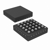
IC CBL DVR DUAL HD/SD 25-UARRAY
Manufacturer
National Semiconductor
Type
Driverr
Datasheet
1.LMH0307GRENOPB.pdf
(16 pages)
Specifications of LMH0307GRE/NOPB
Applications
Amplifiers, Video Distribution
Mounting Type
Surface Mount
Package / Case
25-Micro Array
Lead Free Status / RoHS Status
Lead free / RoHS Compliant
Other names
LMH0307GRETR


Symbol Parameter
DR
t
t
t
t
RL
SMBus AC Specifications
f
t
t
t
t
t
t
t
t
t
t
t
jit
r
OS
SK
SMB
BUF
HD:STA
SU:STA
SU:STO
HD:DAT
SU:DAT
LOW
HIGH
F
R
POR
,t
AC Electrical Characteristics
Over Supply Voltage and Operating Temperature ranges, unless otherwise specified
Note 1: "Absolute Maximum Ratings" are those parameter values beyond which the life and operation of the device cannot be guaranteed. The stating herein of
these maximums shall not be construed to imply that the device can or should be operated at or beyond these values. The table of "Electrical Characteristics"
specifies acceptable device operating conditions.
Note 2: Current flow into device pins is defined as positive. Current flow out of device pins is defined as negative. All voltages are stated referenced to
V
Note 3: Typical values are stated for V
Note 4: Specification is guaranteed by characterization.
Note 5: Output return loss is dependent on board design. The LMH0307 meets this specification on the SD307 evaluation board.
Note 6: Recommended value — Parameter not tested.
Note 7: Recommended maximum capacitive load per bus segment is 400 pF.
f
SDO
SDI
EE
= 0 Volts.
Input Data Rate
Additive Jitter
Output Rise Time, Fall Time
Mismatch in Rise/Fall Time
Duty Cycle Distortion
Output Overshoot
SDO1 to SDO0 Skew
Output Return Loss
Bus Operating Frequency
Bus free time between Stop and
Start Condition
Hold time after (repeated) Start
Condition. After this period, the
first clock is generated.
Repeated Start Condition setup
time
Stop Condition setup time
Data hold time
Data setup time
Clock low period
Clock high period
Clock/Data Fall Time
Clock/Data Rise Time
Time in which device must be
operational after power on
CC
= +3.3V and T
Conditions
2.97 Gbps
1.485 Gbps
270 Mbps
SD/HD = 0, 20% – 80%,
SD/HD = 1, 20% – 80%
SD/HD = 0
SD/HD = 1
SD/HD = 0, 2.97 Gbps,
(Note
SD/HD = 0, 1.485 Gbps,
(Note
SD/HD = 1,
SD/HD = 0,
SD/HD = 1,
SD/HD = 0,
SD/HD = 1,
5 MHz - 1.5 GHz,
1.5 GHz - 3.0 GHz,
At I
A
SPULLUP
= +25°C.
4)
4)
= MAX
(Note
(Note
(Note
(Note
(Note
(Note
4)
4)
4)
4)
4)
(Note
5
5)
5)
Reference
SDI, SDI
SDO, SDO
(Note
3).
Min
400
300
250
4.7
4.0
4.7
4.0
4.7
4.0
15
10
10
Typ
20
18
15
90
2970
1000
Max
130
800
100
100
300
500
30
50
27
30
10
54
50
8
8
www.national.com
Units
Mbps
ps
ps
ps
kHz
ms
dB
dB
ps
ps
ps
ps
ps
ps
ps
ps
ps
µs
µs
µs
µs
ns
ns
µs
µs
ns
ns
%
%
P-P
P-P
P-P
Related parts for LMH0307GRE/NOPB
Image
Part Number
Description
Manufacturer
Datasheet
Request
R

Part Number:
Description:
IC CBL DVR DUAL 3G HD/SD 25-UARY
Manufacturer:
National Semiconductor
Datasheet:

Part Number:
Description:
3 GBPS HD/SD SDI CABLE DRIVER
Manufacturer:
National Semiconductor
Part Number:
Description:
National Semiconductor [8-Bit D/A Converter]
Manufacturer:
National Semiconductor
Datasheet:
Part Number:
Description:
National Semiconductor [Media Coprocessor]
Manufacturer:
National Semiconductor
Datasheet:
Part Number:
Description:
Digitally Controlled Tone and Volume Circuit with Stereo Audio Power Amplifier, Microphone Preamp Stage and National 3D Sound
Manufacturer:
National Semiconductor
Datasheet:
Part Number:
Description:
Digitally Controlled Tone and Volume Circuit with Stereo Audio Power Amplifier, Microphone Preamp Stage and National 3D Sound
Manufacturer:
National Semiconductor
Datasheet:
Part Number:
Description:
AC97 Rev 2 Codec with Sample Rate Conversion and National 3D Sound
Manufacturer:
National Semiconductor
Part Number:
Description:
Manufacturer:
National Semiconductor
Datasheet:
Part Number:
Description:
Manufacturer:
National Semiconductor
Datasheet:
Part Number:
Description:
General Purpose, Low Voltage, Low Power, Rail-to-Rail Output Operational Amplifiers
Manufacturer:
National Semiconductor
Datasheet:
Part Number:
Description:
8-bit 20 MSPS flash A/D converter.
Manufacturer:
National Semiconductor
Datasheet:
Part Number:
Description:
Low Noise Quad Operational Amplifier
Manufacturer:
National Semiconductor
Datasheet:
Part Number:
Description:
Quad Differential Line Receivers
Manufacturer:
National Semiconductor
Datasheet:
Part Number:
Description:
Quad High Speed Trapezoidal? Bus Transceiver
Manufacturer:
National Semiconductor
Datasheet: